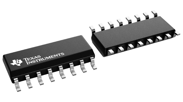
Packaging information
| Package | Pins SOIC (D) | 16 |
| Operating temperature range (°C) -55 to 125 |
| Package qty | Carrier 250 | SMALL T&R |
Features for the CD4521B
- Reset disables the RC oscillator for low-power standby condition
- VDD’ and VSS’ pins are brought out from the crystal oscillator to allow use of external resistors for low-power operation
- Maximum input current of 1 µA at 18 V over full package-temperature range:
100 nA at 18 V and 25°C - Common reset
- 100% tested for 20-V quiescent current
- 5, 10 and 15 V parametric ratings
- Standardized symmetrical output characteristics
- Meets all requirements of JEDEC Tentative Standard No. 13B, "Standard Specifications for Description of ’B’ Series CMOS Devices"
Data sheet acquired from Harris Semiconductor
Description for the CD4521B
CD4521B consists of an oscillator section and 24 ripple-carry binary counter stages. The oscillator configuration (using IN1) allows design of either RC or crystal oscillator circuits. IN1 should be tied either HIGH or LOW when not in use. A HIGH on the RESET causes the counter to go to the all-0’s state and disables the oscillator. The count is advanced on the negative transition of IN1 (and IN2). A time-saving test mode is described in the Functional Test Sequence Table and in Fig. 6.
The CD4521B types are supplied in 16-lead dual-in-line plastic packages (E suffix), 16-lead small-outline packages (M, M96, MT, and NSR suffixes), and 16-lead thin shrink small-outline packages (PW and PWR suffixes).
