Packaging information
| Package | Pins CFP (HSL) (HBD) | 64 |
| Operating temperature range (°C) 25 to 25 |
| Package qty | Carrier 14 | TUBE |
Features for the LMX2615-SP
- Radiation specifications:
- Single event latch-up >120MeV-cm2/mg
- Total ionizing dose to 100krad(Si)
- SMD 5962R1723601VXC
- 40MHz to 15.2GHz output frequency
- –110dBc/Hz phase noise at 100kHz offset with 15GHz carrier
- 45fs RMS jitter at 8GHz (100Hz to 100MHz)
- Programmable output power
- PLL key specifications:
- Figure of merit: –236dBc/Hz
- Normalized 1/f noise: –129dBc/Hz
- Up to 200MHz phase detector frequency
- Synchronization of output phase across multiple devices
- Support for SYSREF with programmable delay
- 3.3V single power supply operation
- 71 pre-selected pin modes
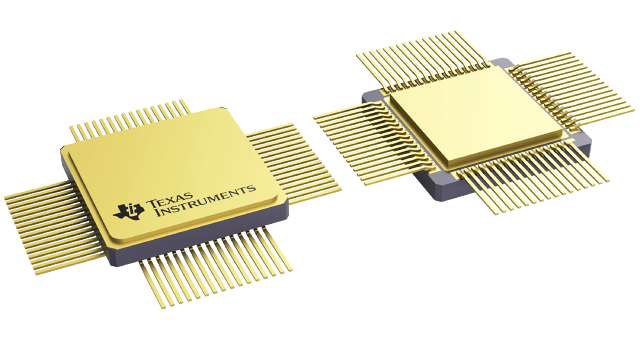
- 11 × 11mm² 64-lead CQFP ceramic package
- Operating temperature range: –55°C to +125°C
Description for the LMX2615-SP
The LMX2615-SP is a high performance wideband phase-locked loop (PLL) with integrated voltage controlled oscillator (VCO) and voltage regulators that can output any frequency from 40MHz and 15.2GHz without a doubler, which eliminates the need for ½ harmonic filters. The VCO on this device covers an entire octave so the frequency coverage is complete down to 40MHz. The high performance PLL with a figure of merit of –236dBc/Hz and high phase detector frequency can attain very low in-band noise and integrated jitter.
The LMX2615-SP allows users to synchronize the output of multiple instances of the device. This means that deterministic phase can be obtained from a device in any use case including the one with fractional engine or output divider enabled. The device also adds support for either generating or repeating SYSREF (compliant to JESD204B standard), making the device designed low-noise clock source for high-speed data converters.