Packaging information
| Package | Pins SOT-23 (DBV) | 5 |
| Operating temperature range (°C) -40 to 125 |
| Package qty | Carrier 3,000 | LARGE T&R |
Features for the LP2982
- VIN range (new chip): 2.5V to 16V
- VOUT range (new chip): 1.2V to 5.0V
- VOUT accuracy:
- ±1% for A-grade (legacy chip)
- ±1.5% for standard-grade (legacy chip)
- ±0.5% (new chip)
- ±1% output accuracy over load and temperature (new chip)
- Output current: Up to 50mA
- Low IQ (new chip): 69µA at ILOAD = 0mA
- Low IQ (new chip): 380µA at ILOAD = 50mA
- Shutdown current:
- 1µA for legacy chip
- 2.25µA for new chip
- Low noise: 30µVRMS with 10nF bypass capacitor
- Output current limiting and thermal protection
- Stable with 2.2µF ceramic capacitors (new chip)
- High PSRR: 70dB at 1kHz, 40dB at 1MHz
- Operating junction temperature: –40°C to +125°C
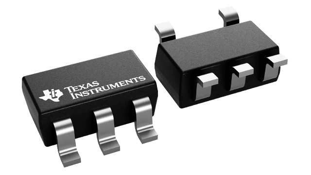
- Package: 5-pin SOT-23 (DBV)
Description for the LP2982
The LP2982 is a fixed-output, wide-input, low-noise, low-dropout voltage regulator supporting an input voltage range from 2.5V to 16V (for new chip) and up to 50mA of load current. The LP2982 supports an output range of 1.2V to 5.0V (new chip).
Additionally, the LP2982 (new chip) has a ±1% output accuracy across load, and temperature that can meet the needs of low-voltage microcontrollers (MCUs) and processors.
Low output noise of 30µVRMS (with 10nF bypass capacitors) and wide bandwidth PSRR performance of greater than 70dB at 1kHz and 40dB at 1MHz help attenuate the switching frequency of an upstream DC/DC converter and minimize post regulator filtering.
The new chip version of the LP2982 includes an internal soft-start mechanism to reduce inrush current during start up, thus minimizing input capacitance requirement. Standard protection features, such as overcurrent and overtemperature protection, are included.
The LP2982 is available in a 5-pin 2.9mm × 2.8mm SOT-23 (DBV) package.