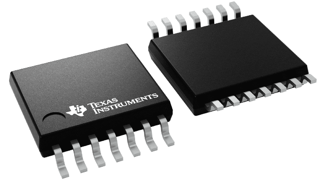
Packaging information
| Package | Pins TSSOP (PW) | 14 |
| Operating temperature range (°C) -40 to 125 |
| Package qty | Carrier 90 | TUBE |
Features for the SN74LVC125A
- 3-State outputs
- Separate OE for all 4 buffers
- Operates from 1.65V to 3.6V
- Specified from –40°C to 85°C and –40°C to 125°C
- Inputs accept voltages to 5.5V
- Max tpd of 4.8ns at 3.3V
- Typical VOLP (output ground bounce) < 0.8V at VCC = 3.3V, TA = 25°C
- Typical VOHV (output VOH undershoot) > 2V at VCC = 3.3V, TA = 25°C
- Latch-up performance exceeds 250mA per JESD 17
Description for the SN74LVC125A
This quadruple bus buffer gate is designed for 1.65V to 3.6V VCC operation.
The SN74LVC125A device features independent line drivers with 3-state outputs. Each output is disabled when the associated output-enable (OE) input is high.
To ensure the high-impedance state during power up or power down, OE should be tied to VCC through a pullup resistor; the minimum value of the resistor is determined by the current-sinking capability of the driver.
Inputs can be driven from either 3.3V or 5V devices. This feature allows the use of this device as a translator in a mixed 3.3V/5V system environment.