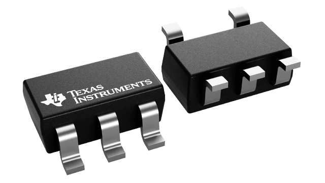
Packaging information
| Package | Pins SOT-23 (DBV) | 5 |
| Operating temperature range (°C) -40 to 125 |
| Package qty | Carrier 3,000 | LARGE T&R |
Features for the SN74LVC1G17
- Available in ultra small 0.64mm2 package (DPW) with 0.5mm pitch
- Supports 5V VCC operation
- Inputs accept voltages to 5.5V
- Maximum tpd of 4.6ns at 3.3V
- Low power consumption, 10µA maximum ICC
- ±24mA output drive at 3.3V
- Ioff supports live insertion, partial-power-down mode, and back-drive protection
- Latch-up performance exceeds 100mA per JESD 78, Class II
- ESD protection exceeds JESD 22
- 2000V human-body model (A114A)
- 200V machine model (A115A)
- 1000V charged-device model (C101)
Description for the SN74LVC1G17
This single Schmitt-trigger buffer is designed for 1.65V to 5.5V VCC operation.
The SN74LVC1G17 device contains one buffer and performs the Boolean function Y = A.
The CMOS device has high output drive while maintaining low static power dissipation over a broad VCC operating range.
The SN74LVC1G17 is available in a variety of packages, including the ultra-small DPW package with a body size of 0.8mm × 0.8mm.
