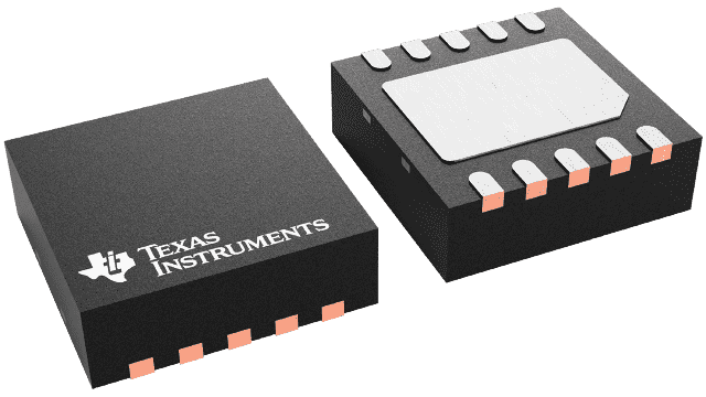
Packaging information
| Package | Pins VSON (DRC) | 10 |
| Operating temperature range (°C) -40 to 125 |
| Package qty | Carrier 250 | SMALL T&R |
Features for the TPS712
- Dual 250 mA High-Performance RF LDOs
- Available in Fixed and Adjustable
Voltage Options (1.2 V to 5.5 V) - High PSRR: 65 dB at 10 kHz
- UltraLow Noise: 32 µVrms
- Fast Start-Up Time: 60 µs
- Stable with 2.2 µF Ceramic Capacitor
- Excellent Load/Line Transient Response
- Very Low Dropout Voltage: 125 mV at 250 mA
- Independent Enable Pins
- Thermal Shutdown and Independent Current Limit
- Available in Thermally-Enhanced SON Package: 3mm × 3mm × 1mm
- APPLICATIONS
- Cellular and Cordless Phones
- Wireless PDA/Handheld Products
- PCMCIA/Wireless LAN Applications
- Digital Camera/Camcorder/Internet Audio
- DSP/FPGA/ASIC/Controllers and Processors
Description for the TPS712
The TPS712xx family of low-dropout (LDO) voltage regulators is tailored to noise-sensitive and RF applications. These products feature dual 250 mA LDOs with ultralow noise, high power-supply rejection ratio (PSRR), and fast transient and start-up response. Each regulator output is stable with low-cost 2.2 µF ceramic output capacitors and features very low dropout voltages (125 mV typical at 250 mA). Each regulator achieves fast start-up times (approximately 60 µs with a 0.001 µF bypass capacitor) while consuming very low quiescent current (300 µA typical with both outputs enabled). When the device is placed in standby mode, the supply current is reduced to less than 0.3 µA typical. Each regulator exhibits approximately 32 µrms of output voltage noise with VOUT = 2.8 V and a 0.01 µF noise reduction (NR) capacitor. Applications with analog components that are noise-sensitive, such as portable RF electronics, will benefit from high PSRR, low noise, and fast line and load transient features. The TPS712 family is offered in a thin 3mm × 3mm SON package and is fully specified from –40°C to +125°C (TJ).
