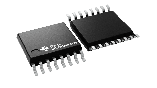
Packaging information
| Package | Pins TSSOP (PW) | 16 |
| Operating temperature range (°C) -40 to 85 |
| Package qty | Carrier 2,000 | LARGE T&R |
Features for the TXB0106
- 1.2V to 3.6V on A port and 1.65 to 5.5V on B Port (VCCA ≤ VCCB)
- VCC isolation feature – if either VCC input is at GND, all outputs are in the high-impedance state
- OE input circuit referenced to VCCA
- Low-power consumption, 4µA max ICC
- Ioff supports partial-power-down mode operation
- Latch-up performance exceeds 100mA per JESD 78, class II
- ESD protection exceeds JESD 22
- A port
- 2500V human body model (A114-B)
- 150V machine model (A115-A)
- 1500V charged-device model (C101)
- B port
- ±15kV human body model (A114-B)
- 150V machine model (A115-A)
- 1500V charged-device model (C101)
- A port
Description for the TXB0106
This 6-bit noninverting translator uses two separate configurable power-supply rails. The A port is designed to track VCCA. VCCA accepts any supply voltage from 1.2V to 3.6V. The B port is designed to track VCCB. VCCB accepts any supply voltage from 1.65V to 5.5V. This allows for universal low-voltage bidirectional translation between any of the 1.2V, 1.5V, 1.8V, 2.5V, 3.3V, and 5V voltage nodes. VCCA must not exceed VCCB.
When the output-enable (OE) input is low, all outputs are placed in the high-impedance state.
The TXB0106 is designed so that the OE input circuit is supplied by VCCA.
This device is fully specified for partial-power-down applications using Ioff. The Ioff circuitry disables the outputs, preventing damaging current backflow through the device during power down.
To verify the high-impedance state during power up or power down, tie the OE to the GND through a pulldown resistor; the minimum value of the resistor is determined by the current-sourcing capability of the driver.