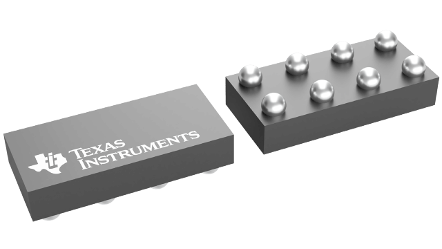
Packaging information
| Package | Pins DSBGA (YZP) | 8 |
| Operating temperature range (°C) -40 to 85 |
| Package qty | Carrier 3,000 | LARGE T&R |
Features for the TXS0102
- No direction-control signal needed
- Maximum data rates:
- 24Mbps (push pull)
- 2Mbps (open drain)
- Available in the Texas Instruments NanoStar™ integrated circuit package
- 1.65V to 3.6V on A port and 2.3V to 5.5V on B port (VCCA ≤ VCCB)
- VCC isolation feature: if either VCC input is at GND, both ports are in the High-Impedance state
- No power-supply sequencing required: either VCCA or VCCB can be ramped first
- Ioff supports partial-power-down mode operation
- Latch-up performance exceeds 100mA per JESD 78, Class II
- ESD protection exceeds JESD 22:
- A port:
- 2500V Human-Body Model (A114-B)
- 250V Machine Model (A115-A)
- 1500V Charged-Device Model (C101)
- B port:
- 8kV Human-Body Model (A114-B)
- 250V Machine Model (A115-A)
- 1500V Charged-Device Model (C101)
- A port:
Description for the TXS0102
This two-bit non-inverting translator is a bidirectional voltage-level translator and can be used to establish digital switching compatibility between mixed-voltage systems. It uses two separate configurable power-supply rails, with the A ports supporting operating voltages from 1.65V to 3.6V while it tracks the VCCA supply, and the B ports supporting operating voltages from 2.3V to 5.5V while it tracks the VCCB supply. This allows the support of both lower and higher logic signal levels while providing bidirectional translation capabilities between any of the 1.8V, 2.5V, 3.3V, and 5V voltage nodes.
When the output-enable (OE) input is low, all I/Os are placed in the high-impedance state, which significantly reduces the power-supply quiescent current consumption.
To put the device in the high-impedance state during power up or power down, tie OE to GND through a pulldown resistor; the current-sourcing capability of the driver determines the minimum value of the resistor.