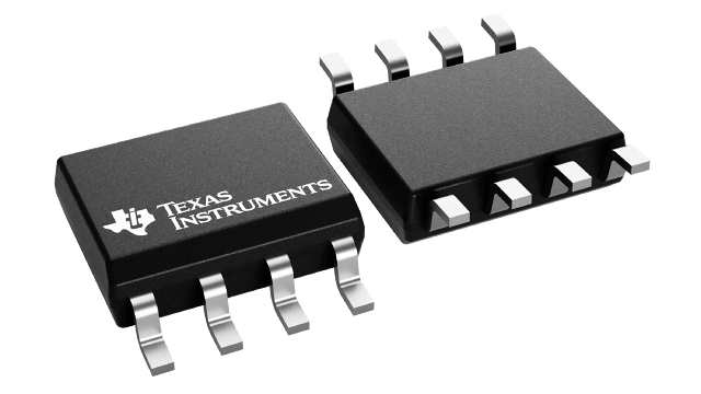
封裝資訊
| 封裝 | 針腳 SOIC (D) | 8 |
| 操作溫度範圍 (°C) -40 to 125 |
| 包裝數量 | 運送業者 2,500 | LARGE T&R |
TLIN1027-Q1 的特色
- AEC-Q100 Qualified for automotive applications
- Temperature grade 1: –40°C to 125°C TA
- Device HBM certification level: ±8 kV
- Device CDM certification level: ±1.5 kV
- Compatible with LIN 2.0, LIN 2.1, LIN 2.2, LIN 2.2 A and ISO/DIS 17987–4.2 (See Switching Characteristics)
- Compatible with SAE J2602 recommended practice for LIN
- Supports ISO 9141 (K-Line)
- Supports 12 V applications
- LIN transmit data rate up to 20-kbps
- Wide operating ranges
- 4-V to 36-V Supply voltage
- ±45-V LIN bus fault protection
- Sleep mode: ultra-low current consumption allows wake-up event from:
- LIN bus
- Local wake up through EN
- No dominant state timeout
- Power up and down glitch free operation
- Protection features:
- Under voltage protection on VSUP
- Thermal shutdown protection
- Unpowered node or ground disconnection failsafe at system level.
- Available in SOIC (8) and leadless VSON (8) packages for improved automated optical inspection (AOI) capability
TLIN1027-Q1 的說明
The TLIN1027-Q1 is a local interconnect network (LIN) physical layer transceiver with integrated wake-up and protection features, compatible with LIN 2.0, LIN 2.1, LIN 2.2, LIN 2.2 A and ISO/DIS 17987–4.2 standards. LIN is a single-wire bidirectional bus typically used for in-vehicle networks using data rates up to 20 kbps. The TLIN1027-Q1 is designed to support 12-V applications with wider operating voltage and additional bus-fault protection.
The LIN receiver supports data rates up to 100 kbps for faster in-line programming. The TLIN1027-Q1 converts the data stream on the TXD input into a LIN bus signal using a current-limited wave-shaping driver which reduces electromagnetic emissions (EME). The receiver converts the data stream to logic level signals that are sent to the microprocessor through the open-drain RXD pin. Ultra-low current consumption is possible using the sleep mode which allows wake-up through LIN bus or EN pin.
