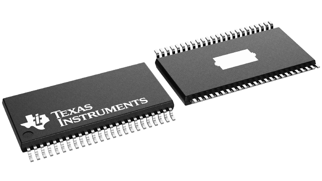
封裝資訊
| 封裝 | 針腳 HTSSOP (DCA) | 48 |
| 操作溫度範圍 (°C) -40 to 125 |
| 包裝數量 | 運送業者 2,000 | SMALL T&R |
TPIC71002-Q1 的特色
- Two-Channel Squib Drivers For Airbag Application
- Loop Diagnostics Monitor and Reporting
- Two Logic Inputs Providing Independent Safety Logic for
Enabling/Disabling Deployment - Two Independent Thermally Protected High-Side Drivers that Can
Source Deployment or Diagnostic Current Level to Each Squib Load - Two Independent Avalanche Voltage and Thermally Protected Low-Side
Drivers that can Sink Deployment or Diagnostic Current Level
from Each Squib Load - Each Output Capable of 1.2 A/1.75 A Firing Current for Typical 2 ms/0.5 ms
- SPI Slave Interface for Serial Bus Communication with Parity Check
- Firing VZx Voltage Range 10V to 35V, Transients up to 40 V
- Programmable Firing Time up to 8.2 ms
- Common Load Current Settings for All Deployment Loops, Using Registers
- Individual Firing Current Timer Limit Set for Each Deployment Loop, Using Registers
- Firing Current Timer to Monitor Firing Current Over Deployment Time for Each Deployment Loop
- Independent Switch Control for Both High- And Low-Side Switches
- Diagnostic Mode for Fault Checking
- Internal Fault Monitoring for Safe Operation
- Multiplexable Output Buffer for Analog Voltage Measurements
- Use of External Clamping Devices on Squib Pins is Not Required to Protect the
Deployment ASIC Against Substrate Injection Effects During Deployment Due to Dynamic
Shorts to Ground - External Pin Connection to the Microprocessor ADC Supply for Ratio-Metric Squib
Resistance Measurement - 40-V Pin Capability on All Pins (Except GNDx, AGND, DGND, VCC5, VDDIO, AMX_OUT)
- Operating Ambient Temperature Range: –40°C to 105°C
- Thermally Enhanced 48-Pin TSSOP DCA PowerPad™ Package
- APPLICATIONS
- Squib Drivers for Airbag Application
TPIC71002-Q1 的說明
The TPIC71002 is a two-channel squib driver for airbag deployment in automotive applications. Each channel consists of a high side and a low side switches with independent control logic for protection against inadvertent deployment. Both the high and the low side switches have internal current limits and over-temperature protection.
The IC registers are used for two channel configuration, control and status monitoring. To prevent inadvertent deployment, the high and the low side switches are turned on only if the proper configuration sequence is used, two independent arming/safing inputs are active and multiple inputs to the deploy controller logic are at the correct level. The registers are programmed using a serial communication interface.
To prevent excessive power dissipation the maximum active ON time for each channel is limited by programmable Firing Time Out Timer. In addition, a current limit register is used to program the maximum current through the switches during a deployment. The current limitation on the low side switch is larger than the corresponding high side switch. During deployment, the low side switch will be fully enhanced and operates in RDS_ON mode and the high side switch will be in the current regulation mode.
IC diagnostic functions monitor deployment pin voltages to facilitate high-side switch test, low-side switch test, squib resistance measurements, squib leakage measurement to battery or ground or leakage between any squib channels. The squib leakage measurement does not require the squib load to be present and covers both Zx and ZMx pins. Diagnostic information is communicated through the AMX_OUT pin (for analog signals) and SPI mapped status registers (for status signals latched in digital core).
The high-side and low-side squib drivers have a diagnostic level current limit and a deployment level current limit. The default current limit for high-side and low-side squib drivers is the diagnostic level current limit. The high-side switch deployment current limit for all high-side drivers can be set to either 1.2 A min or 1.75 A min (see Table 1) through SPI mapped registers and device EEPROM settings (see Table 2). The low-side switch deployment current limit is not programmable and is fixed to a level greater than the high-side driver current limit. The ON time duration for each individual squib driver can be programmed through SPI mapped registers.
The deployment sequence requires a specific set of software commands combined with external hardware arming/safing logic inputs (TZ=H, IWD=L) to provide deployment capability. The turn-on sequence of the high-side and low-side drivers is software controlled via SPI commands. The turn-off procedure is automatically controlled by the deployment ASIC for the high side drivers, while the low side drivers turn-off procedure can be controlled by the deployment ASIC or by software via SPI commands. After the programmed ON time deployment has been achieved, the high-side driver is deactivated first. It is followed by the low-side driver deactivation after approximately 100usec (in case of hardware control turn-off sequence device configuration), or after SPI command for low side driver turn-off has been received from an external microcontroller (in case of software control turn-off sequence device configuration).
The RESET_N is an active low input reset signal. This input is driven high (by the power supply unit and/or the external µC) once the external voltage supplies are within the specified limits. The external microcontroller is required to configure and control device through the serial communication interface. Reliable software is critical for the system operation.
Extended deployment duration activates the over-temperature protection circuit and terminates deployment. If short-to-ground condition occurs during deployment, 35-V firing voltage is completely dropped across the HS_FET, thereby thermal shut down protection kicks in to protect the device.
