SBASAF6A October 2021 – October 2024 ADC09DJ1300 , ADC09QJ1300 , ADC09SJ1300
PRODUCTION DATA
- 1
- 1 Features
- 2 Applications
- 3 Description
- 4 Pin Configuration and Functions
-
5 Specifications
- 5.1 Absolute Maximum Ratings
- 5.2 ESD Ratings
- 5.3 Recommended Operating Conditions
- 5.4 Thermal Information
- 5.5 Electrical Characteristics: DC Specifications
- 5.6 Electrical Characteristics: Power Consumption
- 5.7 Electrical Characteristics: AC Specifications
- 5.8 Timing Requirements
- 5.9 Switching Characteristics
- 5.10 Typical Characteristics
-
6 Detailed Description
- 6.1 Overview
- 6.2 Functional Block Diagram
- 6.3
Feature Description
- 6.3.1 Device Comparison
- 6.3.2 Analog Input
- 6.3.3 ADC Core
- 6.3.4
Clocking
- 6.3.4.1 Converter PLL (C-PLL) for Sampling Clock Generation
- 6.3.4.2 LVDS Clock Outputs (PLLREFO±, TRIGOUT±)
- 6.3.4.3 Optional CMOS Clock Outputs (ORC, ORD)
- 6.3.4.4 SYSREF for JESD204C Subclass-1 Deterministic Latency
- 6.3.4.5
JESD204C Interface
- 6.3.4.5.1 Transport Layer
- 6.3.4.5.2 Scrambler
- 6.3.4.5.3 Link Layer
- 6.3.4.5.4 8B/10B Link Layer
- 6.3.4.5.5 64B/66B Link Layer
- 6.3.4.5.6 Physical Layer
- 6.3.4.5.7 JESD204C Enable
- 6.3.4.5.8 Multi-Device Synchronization and Deterministic Latency
- 6.3.4.5.9 Operation in Subclass 0 Systems
- 6.3.4.5.10 Alarm Monitoring
- 6.4
Device Functional Modes
- 6.4.1 Low Power Mode and High Performance Mode
- 6.4.2 JESD204C Modes
- 6.4.3 Power-Down Modes
- 6.4.4
Test Modes
- 6.4.4.1 Serializer Test-Mode Details
- 6.4.4.2 PRBS Test Modes
- 6.4.4.3 Clock Pattern Mode
- 6.4.4.4 Ramp Test Mode
- 6.4.4.5 Short and Long Transport Test Mode
- 6.4.4.6 D21.5 Test Mode
- 6.4.4.7 K28.5 Test Mode
- 6.4.4.8 Repeated ILA Test Mode
- 6.4.4.9 Modified RPAT Test Mode
- 6.4.4.10 Calibration Modes and Trimming
- 6.4.4.11 Offset Calibration
- 6.4.4.12 Trimming
- 6.5 Programming
- 6.6 SPI_Register_Map Registers
- 7 Application and Implementation
- 8 Device and Documentation Support
- 9 Revision History
- 10Mechanical, Packaging, and Orderable Information
Package Options
Mechanical Data (Package|Pins)
- AAV|144
Thermal pad, mechanical data (Package|Pins)
Orderable Information
6.4.4.10 Calibration Modes and Trimming
The device has two calibration modes available: foreground calibration and background calibration. When foreground calibration is initiated the ADCs are taken offline to calibrate and the output data becomes mid-code (0x000 in 2's complement) until calibration is finished. Background calibration allows the ADC to continue normal operation while the ADC cores are calibrated in the background by swapping in a different ADC core to take its place. Additional offset calibration features are available in both foreground and background calibration modes. Further, a number of ADC parameters can be trimmed to optimize performance in a user system.
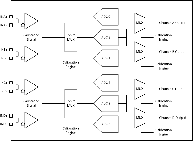
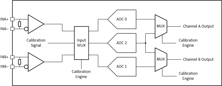
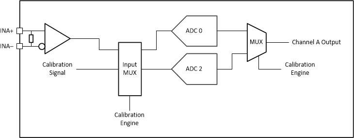
The device consists of a total of six ADC cores. In foreground calibration mode ADC 0 samples INA±, ADC 1 samples INB±, ADC 4 samples INC± and ADC 5 samples IND±. In the background calibration modes, ADC core 2 is swapped in periodically for ADC 0 and ADC 1 and ADC core 3 is swapped in periodically for ADC 4 and 5 so that they can be calibrated without disrupting operation. Figure 6-15 through Figure 6-17 provide a diagrams of the calibration system including labeling of the ADC cores. When calibration is performed the linearity, gain, and offset voltage for each bank are calibrated to an internally generated calibration signal. The analog inputs can be driven during calibration, both foreground and background, except that when offset calibration (OS_CAL or BGOS_CAL) is used there must be no signals (or aliased signals) near DC for proper estimation of the offset (see the Offset Calibration section).
 Figure 6-15 Quad Channel Calibration System Block Diagram
 Figure 6-16 DualChannel Calibration System Block Diagram
 Figure 6-17 Single Channel Calibration System Block Diagram
In addition to calibration, a number of ADC parameters are user controllable to provide trimming for optimal performance. These parameters include input offset voltage, ADC gain and input termination resistance. The default trim values are programmed at the factory to unique values for each device that are determined to be optimal at the test system operating conditions. The user can read the factory-programmed values from the trim registers and adjust as desired. The register fields that control the trimming are labeled according to the input that is being sampled (INA±, INB±, INC± or IND±) and the ADC core that is being trimmed. The user is not expected to change the trim values as operating conditions change, however the user can change values as needed. Any custom trimming must be done on a per device basis because of process variations, meaning that there is no global optimal setting for all parts. See the Trimming section for information about the available trim parameters and associated registers.