SLVSDR2B November 2018 – March 2021 ADC12DJ3200QML-SP
PRODUCTION DATA
- 1 Features
- 2 Applications
- 3 Description
- 4 Revision History
- 5 Pin Configuration and Functions
-
6 Specifications
- 6.1 Absolute Maximum Ratings
- 6.2 ESD Ratings
- 6.3 Recommended Operating Conditions
- 6.4 Thermal Information
- 6.5 Electrical Characteristics: DC Specifications
- 6.6 Electrical Characteristics: Power Consumption
- 6.7 Electrical Characteristics: AC Specifications (Dual-Channel Mode)
- 6.8 Electrical Characteristics: AC Specifications (Single-Channel Mode)
- 6.9 Timing Requirements
- 6.10 Switching Characteristics
- 6.11 Timing Diagrams
- 6.12 Typical Characteristics
-
7 Detailed Description
- 7.1 Overview
- 7.2 Functional Block Diagram
- 7.3
Feature Description
- 7.3.1 Analog Inputs
- 7.3.2 ADC Core
- 7.3.3 Timestamp
- 7.3.4 Clocking
- 7.3.5 Digital Down Converters (Dual-Channel Mode Only)
- 7.3.6 JESD204B Interface
- 7.3.7 Alarm Monitoring
- 7.3.8 Temperature Monitoring Diode
- 7.3.9 Analog Reference Voltage
- 7.4
Device Functional Modes
- 7.4.1 Dual-Channel Mode
- 7.4.2 Single-Channel Mode (DES Mode)
- 7.4.3 JESD204B Modes
- 7.4.4 Power-Down Modes
- 7.4.5 Test Modes
- 7.4.6 Calibration Modes and Trimming
- 7.4.7 Offset Calibration
- 7.4.8 Trimming
- 7.4.9 Offset Filtering
- 7.5 Programming
- 7.6 Register Maps
- 8 Application Information Disclaimer
- 9 Layout
- 10Device and Documentation Support
Package Options
Refer to the PDF data sheet for device specific package drawings
Mechanical Data (Package|Pins)
- ZMX|196
- NWE|196
Thermal pad, mechanical data (Package|Pins)
Orderable Information
7.3.5 Digital Down Converters (Dual-Channel Mode Only)
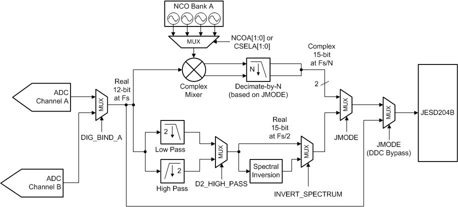
After converting the analog voltage to a digital value, the digitized sample can either be sent directly to the JESD204B interface block (DDC bypass) or sent to the digital down conversion (DDC) block for frequency conversion and decimation (in dual-channel mode only). Frequency conversion and decimation allow a specific frequency band to be selected and output in the digital data stream while reducing the effective data rate and interface speed or width. The DDC is designed such that the digital processing does not degrade the noise spectral density (NSD) performance of the ADC. Figure 7-5 illustrates the digital down converter for channel A of the ADC12DJ3200QML-SP. Channel B has the same structure with the input data selected by DIG_BIND_B and the NCO selection mux controlled by pins NCOB[1:0] or through CSELB[1:0].
 Figure 7-5 Channel A Digital Down Conversion Block (Dual-Channel Mode Only)