SLVSEN9F April 2019 – June 2024 ADC12DJ5200RF
PRODUCTION DATA
- 1
- 1 Features
- 2 Applications
- 3 Description
- 4 Pin Configuration and Functions
-
5 Specifications
- 5.1 Absolute Maximum Ratings
- 5.2 ESD Ratings
- 5.3 Recommended Operating Conditions
- 5.4 Thermal Information
- 5.5 Electrical Characteristics: DC Specifications
- 5.6 Electrical Characteristics: Power Consumption
- 5.7 Electrical Characteristics: AC Specifications (Dual-Channel Mode)
- 5.8 Electrical Characteristics: AC Specifications (Single-Channel Mode)
- 5.9 Timing Requirements
- 5.10 Switching Characteristics
- 5.11 Typical Characteristics
-
6 Detailed Description
- 6.1 Overview
- 6.2 Functional Block Diagram
- 6.3
Feature Description
- 6.3.1 Device Comparison
- 6.3.2 Analog Inputs
- 6.3.3 ADC Core
- 6.3.4 Temperature Monitoring Diode
- 6.3.5 Timestamp
- 6.3.6 Clocking
- 6.3.7 Programmable FIR Filter (PFIR)
- 6.3.8 Digital Down Converters (DDC)
- 6.3.9
JESD204C Interface
- 6.3.9.1 Transport Layer
- 6.3.9.2 Scrambler
- 6.3.9.3 Link Layer
- 6.3.9.4 8B/10B Link Layer
- 6.3.9.5
64B/66B Link Layer
- 6.3.9.5.1 64B/66B Encoding
- 6.3.9.5.2 Multiblocks, Extended Multiblocks and the Local Extended Multiblock Clock (LEMC)
- 6.3.9.5.3 Block, Multiblock and Extended Multiblock Alignment using Sync Header
- 6.3.9.5.4 Initial Lane Alignment
- 6.3.9.5.5 Block, Multiblock and Extended Multiblock Alignment Monitoring
- 6.3.9.6 Physical Layer
- 6.3.9.7 JESD204C Enable
- 6.3.9.8 Multi-Device Synchronization and Deterministic Latency
- 6.3.9.9 Operation in Subclass 0 Systems
- 6.3.10 Alarm Monitoring
- 6.4
Device Functional Modes
- 6.4.1 Dual-Channel Mode
- 6.4.2 Single-Channel Mode (DES Mode)
- 6.4.3 Dual-Input Single-Channel Mode (DUAL DES Mode)
- 6.4.4 JESD204C Modes
- 6.4.5 Power-Down Modes
- 6.4.6 Test Modes
- 6.4.7 Calibration Modes and Trimming
- 6.4.8 Offset Calibration
- 6.4.9 Trimming
- 6.5 Programming
- 6.6 SPI Register Map
- 7 Application Information Disclaimer
- 8 Device and Documentation Support
- 9 Revision History
- 10Mechanical, Packaging, and Orderable Information
Package Options
Mechanical Data (Package|Pins)
- ZEG|144
- AAV|144
Thermal pad, mechanical data (Package|Pins)
Orderable Information
6.3.2 Analog Inputs
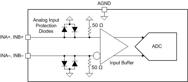
The analog inputs of the device have internal buffers to enable high input bandwidth and to isolate sampling capacitor glitch noise from the input circuit. Analog inputs must be driven differentially because operation with a single-ended signal results in degraded performance. Both AC-coupling and DC-coupling of the analog inputs is supported. The analog inputs are designed for an input common-mode voltage (VCMI) of 0 V, which is terminated internally through single-ended, 50-Ω resistors to ground (GND) on each input pin. DC-coupled input signals must have a common-mode voltage that meets the device input common-mode requirements specified as VCMI in the Recommended Operating Conditions table. The 0-V input common-mode voltage simplifies the interface to split-supply, fully-differential amplifiers and to a variety of transformers and baluns. The device includes internal analog input protection to protect the ADC inputs during overranged input conditions; see the Analog Input Protection section. Figure 6-1 provides a simplified analog input model.
 Figure 6-1 ADC12DJ5200RF Analog Input Internal Termination and Protection Diagram
There is minimal degradation in analog input bandwidth when using single-channel mode versus dual-channel mode. Either analog input (INA+ and INA– or INB+ and INB–) can be used in single-channel mode. The desired input can be chosen using SINGLE_INPUT in the input mux control register. A calibration needs to be performed after switching the input mux for the changes to take effect. Further, two inputs can be used in single-channel mode to drive the interleaved ADCs separately using the SINGLE_INPUT register setting. This mode is called dual-input single-channel mode. Dual-input single-channel mode is equivalent to dual channel mode, except ADC B samples out-of-phase with ADC A (single-channel mode sample timing). This mode is available when a single-channel mode JMODE setting is chosen.