SBAS672E July 2014 – June 2022 ADC3221 , ADC3222 , ADC3223 , ADC3224
PRODUCTION DATA
- 1 Features
- 2 Applications
- 3 Description
- 4 Revision History
- 5 Pin Configuration and Functions
-
6 Specifications
- 6.1 Absolute Maximum Ratings
- 6.2 ESD Ratings
- 6.3 Recommended Operating Conditions (1)
- 6.4 Thermal Information
- 6.5 Electrical Characteristics: General
- 6.6 Electrical Characteristics: ADC3221, ADC3222
- 6.7 Electrical Characteristics: ADC3223, ADC3224
- 6.8 AC Performance: ADC3221
- 6.9 AC Performance: ADC3222
- 6.10 AC Performance: ADC3223
- 6.11 AC Performance: ADC3224
- 6.12 Digital Characteristics
- 6.13 Timing Requirements: General
- 6.14 Timing Requirements: LVDS Output
- 6.15 Typical Characteristics: ADC3221
- 6.16 Typical Characteristics: ADC3222
- 6.17 Typical Characteristics: ADC3223
- 6.18 Typical Characteristics: ADC3224
- 6.19 Typical Characteristics: Common
- 6.20 Typical Characteristics: Contour
- 7 Parameter Measurement Information
-
8 Detailed Description
- 8.1 Overview
- 8.2 Functional Block Diagram
- 8.3 Feature Description
- 8.4 Device Functional Modes
- 8.5 Programming
- 8.6
Register Maps
- 8.6.1 Summary of Special Mode Registers
- 8.6.2
Serial Register Description
- 8.6.2.1 Register 01h
- 8.6.2.2 Register 03h
- 8.6.2.3 Register 04h
- 8.6.2.4 Register 05h
- 8.6.2.5 Register 06h
- 8.6.2.6 Register 07h
- 8.6.2.7 Register 09h
- 8.6.2.8 Register 0Ah
- 8.6.2.9 Register 0Bh
- 8.6.2.10 Register 0Eh
- 8.6.2.11 Register 0Fh
- 8.6.2.12 Register 13h
- 8.6.2.13 Register 15h
- 8.6.2.14 Register 25h
- 8.6.2.15 Register 27h
- 8.6.2.16 Register 41Dh
- 8.6.2.17 Register 422h
- 8.6.2.18 Register 434h
- 8.6.2.19 Register 439h
- 8.6.2.20 Register 51Dh
- 8.6.2.21 Register 522h
- 8.6.2.22 Register 534h
- 8.6.2.23 Register 539h
- 8.6.2.24 Register 608h
- 8.6.2.25 Register 70Ah
- 9 Applications and Implementation
- 10Device and Documentation Support
- 11Mechanical, Packaging, and Orderable Information
Package Options
Mechanical Data (Package|Pins)
- RGZ|48
Thermal pad, mechanical data (Package|Pins)
- RGZ|48
Orderable Information
8.5.1.1.1 Serial Register Write
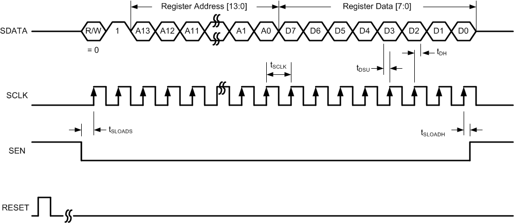
The device internal register can be programmed with these steps:
- Drive the SEN pin low,
- Set the R/W bit to 0 (bit A15 of the 16-bit address),
- Set bit A14 in the address field to 1,
- Initiate a serial interface cycle by specifying the address of the register (A13 to A0) whose content must be written, and
- Write the 8-bit data that are latched in on the SCLK rising edge.
Figure 8-13 and Table 8-4 show the timing requirements for the serial register write operation.
 Figure 8-13 Serial Register Write Timing Diagram
Table 8-4 Serial Interface Timing(1)
| MIN | TYP | MAX | UNIT | ||
|---|---|---|---|---|---|
| fSCLK | SCLK frequency (equal to 1 / tSCLK) | > dc | 20 | MHz | |
| tSLOADS | SEN to SCLK setup time | 25 | ns | ||
| tSLOADH | SCLK to SEN hold time | 25 | ns | ||
| tDSU | SDIO setup time | 25 | ns | ||
| tDH | SDIO hold time | 25 | ns | ||
(1) Typical values are at 25°C, full temperature range is from TMIN = –40°C to TMAX = 85°C, and AVDD = DVDD = 1.8 V, unless otherwise noted.