SBAS683B August 2014 – May 2020 ADS1120-Q1
PRODUCTION DATA.
- 1 Features
- 2 Applications
- 3 Description
- 4 Revision History
- 5 Pin Configuration and Functions
- 6 Specifications
- 7 Parameter Measurement Information
-
8 Detailed Description
- 8.1 Overview
- 8.2 Functional Block Diagram
- 8.3
Feature Description
- 8.3.1 Multiplexer
- 8.3.2 Low-Noise PGA
- 8.3.3 Modulator
- 8.3.4 Digital Filter
- 8.3.5 Output Data Rate
- 8.3.6 Voltage Reference
- 8.3.7 Clock Source
- 8.3.8 Excitation Current Sources
- 8.3.9 Low-Side Power Switch
- 8.3.10 Sensor Detection
- 8.3.11 System Monitor
- 8.3.12 Offset Calibration
- 8.3.13 Power Supplies
- 8.3.14 Temperature Sensor
- 8.4 Device Functional Modes
- 8.5 Programming
- 8.6 Register Map
- 9 Application and Implementation
- 10Power Supply Recommendations
- 11Layout
- 12Device and Documentation Support
- 13Mechanical, Packaging, and Orderable Information
Package Options
Mechanical Data (Package|Pins)
- PW|16
Thermal pad, mechanical data (Package|Pins)
Orderable Information
8.3.2.1 PGA Common-Mode Voltage Requirements
To stay within the linear operating range of the PGA, the input signals must meet certain requirements that are discussed in this section.
The outputs of both amplifiers (A1 and A2) in Figure 39 can not swing closer to the supplies (AVSS and AVDD) than 200 mV. If the outputs OUTP and OUTN are driven to within 200 mV of the supply rails, the amplifiers saturate and consequently become nonlinear. To prevent this nonlinear operating condition the output voltages must meet Equation 7:
Translating the requirements of Equation 7 into requirements referred to the PGA inputs (AINP and AINN) is beneficial because there is no direct access to the outputs of the PGA. The PGA employs a symmetrical design, therefore the common-mode voltage at the output of the PGA can be assumed to be the same as the common-mode voltage of the input signal, as shown in Figure 40.
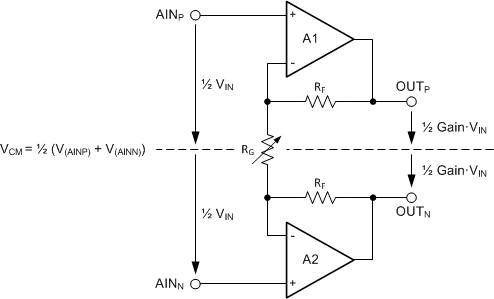 Figure 40. PGA Common-Mode Voltage
 The common-mode voltage is calculated using Equation 8:
The voltages at the PGA inputs (AINP and AINN) can be expressed as Equation 9 and Equation 10:
The output voltages (V(OUTP) and V(OUTN)) can then be calculated as Equation 11 and Equation 12:
The requirements for the output voltages of amplifiers A1 and A2 (Equation 7) can now be translated into requirements for the input common-mode voltage range using Equation 11 and Equation 12, which are given in Equation 13 and Equation 14:
In order to calculate the minimum and maximum common-mode voltage limits, the maximum differential input voltage (VIN (MAX)) that occurs in the application must be used. VIN (MAX) can be less than the maximum possible FS value.
In addition to Equation 13, the minimum VCM must also meet Equation 15 because of the specific design implementation of the PGA.
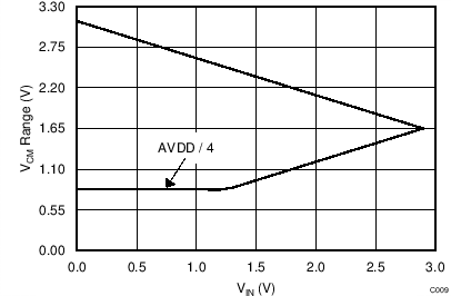
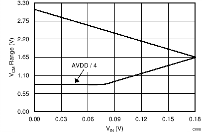
Figure 41 and Figure 42 show a graphical representation of the common-mode voltage limits for AVDD = 3.3 V and AVSS = 0 V, with gain = 1 and gain = 16, respectively.
| AVDD = 3.3 V |
| AVDD = 3.3 V |
The following discussion explains how to apply Equation 13 through Equation 15 to a hypothetical application. The setup for this example is AVDD = 3.3 V, AVSS = 0 V, and gain = 16, using an external reference,
VREF = 2.5 V. The maximum possible differential input voltage VIN = (V(AINP) – V(AINN)) that can be applied is then limited to the full-scale range of FSR = ±2.5 V / 16 = ±0.156 V. Consequently, Equation 13 through Equation 15 yield an allowed VCM range of 1.45 V ≤ VCM ≤ 1.85 V.
If the sensor signal connected to the inputs in this hypothetical application does not make use of the entire full-scale range but is limited to VIN (MAX) = ±0.1 V, for example, then this reduced input signal amplitude relaxes the VCM restriction to 1.0 V ≤ VCM ≤ 2.3 V.
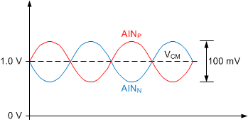
In the case of a fully-differential sensor signal, each input (AINP, AINN) can swing up to ±50 mV around the common-mode voltage (V(AINP) + V(AINN)) / 2, which must remain between the limits of 1.0 V and 2.3 V. The output of a symmetrical wheatstone bridge is an example of a fully-differential signal. Figure 43 shows a situation where the common-mode voltage of the input signal is at the lowest limit. V(OUTN) is exactly at 0.2 V in this case. Any further decrease in common-mode voltage (VCM) or increase in differential input voltage (VIN) drives V(OUTN) below 0.2 V and saturates amplifier A2.
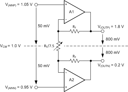 Figure 43. Example where VCM is at Lowest Limit
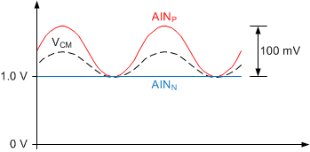
 In contrast, the signal of an RTD is of a pseudo-differential nature (if implemented as shown in the RTD Measurement section), where the negative input is held at a constant voltage other than 0 V and only the voltage on the positive input changes. When a pseudo-differential signal must be measured, the negative input in this example must be biased at a voltage between 0.95 V and 2.25 V. The positive input can then swing up to
VIN (MAX) = 100 mV above the negative input. Note that in this case the common-mode voltage changes at the same time the voltage on the positive input changes. That is, while the input signal swings between 0 V ≤ VIN ≤ VIN (MAX), the common-mode voltage swings between V(AINN) ≤ VCM ≤ V(AINN) + ½ VIN (MAX). Satisfying the common-mode voltage requirements for the maximum input voltage VIN (MAX) ensures the requirements are met throughout the entire signal range.
Figure 44 and Figure 45 show examples of both fully-differential and pseudo-differential signals, respectively.
NOTE
Remember, common-mode voltage requirements with PGA enabled (Equation 13 to Equation 15) are as follows:
- VCM (MIN) ≥ AVSS + ¼ (AVDD – AVSS)
- VCM (MIN) ≥ AVSS + 0.2 V + ½ Gain · VIN (MAX)
- VCM (MAX) ≤ AVDD – 0.2 V – ½ Gain · VIN (MAX)