SBAS661C February 2015 – May 2021 ADS1262 , ADS1263
PRODUCTION DATA
- 1 Features
- 2 Applications
- 3 Description
- 4 Revision History
- 5 Device Comparison
- 6 Pin Configuration and Functions
- 7 Specifications
-
8 Parameter Measurement Information
- 8.1 Offset Temperature Drift Measurement
- 8.2 Gain Temperature Drift Measurement
- 8.3 Common-Mode Rejection Ratio Measurement
- 8.4 Power-Supply Rejection Ratio Measurement
- 8.5 Crosstalk Measurement (ADS1263)
- 8.6 Reference-Voltage Temperature-Drift Measurement
- 8.7 Reference-Voltage Thermal-Hysteresis Measurement
- 8.8 Noise Performance
-
9 Detailed Description
- 9.1 Overview
- 9.2 Functional Block Diagram
- 9.3
Feature Description
- 9.3.1 Multifunction Analog Inputs
- 9.3.2 Analog Input Description
- 9.3.3 Sensor Bias
- 9.3.4 Temperature Sensor
- 9.3.5 Power-Supply Monitor
- 9.3.6 PGA
- 9.3.7 PGA Voltage Overrange Monitors
- 9.3.8 ADC Reference Voltage
- 9.3.9 ADC1 Modulator
- 9.3.10 Digital Filter
- 9.3.11 Sensor-Excitation Current Sources (IDAC1 and IDAC2)
- 9.3.12 Level-Shift Voltage
- 9.3.13 General-Purpose Input/Output (GPIO)
- 9.3.14 Test DAC (TDAC)
- 9.3.15 ADC2 (ADS1263)
- 9.4
Device Functional Modes
- 9.4.1 Conversion Control
- 9.4.2 Conversion Latency
- 9.4.3 Programmable Time Delay
- 9.4.4 Serial Interface
- 9.4.5 Data Ready Pin (DRDY)
- 9.4.6 Conversion Data Software Polling
- 9.4.7 Read Conversion Data
- 9.4.8 ADC Clock Modes
- 9.4.9
Calibration
- 9.4.9.1 Offset and Full-Scale Calibration
- 9.4.9.2 ADC1 Offset Self-Calibration (SFOCAL1)
- 9.4.9.3 ADC1 Offset System Calibration (SYOCAL1)
- 9.4.9.4 ADC2 Offset Self-Calibration ADC2 (SFOCAL2)
- 9.4.9.5 ADC2 Offset System Calibration ADC2 (SYOCAL2)
- 9.4.9.6 ADC1 Full-Scale System Calibration (SYGCAL1)
- 9.4.9.7 ADC2 Full-Scale System Calibration ADC2 (SYGCAL2)
- 9.4.9.8 Calibration Command Procedure
- 9.4.9.9 User Calibration Procedure
- 9.4.10 Reset
- 9.4.11 Power-Down Mode
- 9.4.12 Chop Mode
- 9.5 Programming
- 9.6
Register Maps
- 9.6.1 Device Identification Register (address = 00h) [reset = x]
- 9.6.2 Power Register (address = 01h) [reset = 11h]
- 9.6.3 Interface Register (address = 02h) [reset = 05h]
- 9.6.4 Mode0 Register (address = 03h) [reset = 00h]
- 9.6.5 Mode1 Register (address = 04h) [reset = 80h]
- 9.6.6 Mode2 Register (address = 05h) [reset = 04h]
- 9.6.7 Input Multiplexer Register (address = 06h) [reset = 01h]
- 9.6.8 Offset Calibration Registers (address = 07h, 08h, 09h) [reset = 00h, 00h, 00h]
- 9.6.9 Full-Scale Calibration Registers (address = 0Ah, 0Bh, 0Ch) [reset = 40h, 00h, 00h]
- 9.6.10 IDACMUX Register (address = 0Dh) [reset = BBh]
- 9.6.11 IDACMAG Register (address = 0Eh) [reset = 00h]
- 9.6.12 REFMUX Register (address = 0Fh) [reset = 00h]
- 9.6.13 TDACP Control Register (address = 10h) [reset = 00h]
- 9.6.14 TDACN Control Register (address = 11h) [reset = 00h]
- 9.6.15 GPIO Connection Register (address = 12h) [reset = 00h]
- 9.6.16 GPIO Direction Register (address = 13h) [reset = 00h]
- 9.6.17 GPIO Data Register (address = 14h) [reset = 00h]
- 9.6.18 ADC2 Configuration Register (address = 15h) [reset = 00h]
- 9.6.19 ADC2 Input Multiplexer Register (address = 16h) [reset = 01h]
- 9.6.20 ADC2 Offset Calibration Registers (address = 17h, 18h) [reset = 00h, 00h]
- 9.6.21 ADC2 Full-Scale Calibration Registers (address = 19h, 1Ah) [reset = 00h, 40h]
- 10Application and Implementation
- 11Power Supply Recommendations
- 12Layout
- 13Device and Documentation Support
Package Options
Mechanical Data (Package|Pins)
- PW|28
Thermal pad, mechanical data (Package|Pins)
Orderable Information
9.4.5 Data Ready Pin (DRDY)
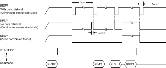
The DRDY pin is an output that transitions low to indicate when ADC1 conversion data are ready for retrieval. Figure 9-42 depicts the DRDY operation. Initially, DRDY is high at power-on. When converting, the state of DRDY depends on the conversion mode (continuous or pulse) and whether the conversion data are retrieved or not. In Continuous conversion mode, after DRDY goes low, DRDY is driven high on the first SCLK falling edge. If data are not read, DRDY remains low and then pulses high 16 fCLK cycles before the next DRDY falling edge. The data must be retrieved before the next DRDY falling edge otherwise the data are overwritten by new data and previous data are lost. In Pulse mode, DRDY is driven high when a conversion is started and goes low when the conversion data are ready. DRDY remains low until the next conversion is started.
The DOUT/DRDY output operates similarly to DRDY. DOUT/DRDY transitions low when ADC1 conversion data are ready. If data are not retrieved, the DOUT/DRDY pin stays low and is pulsed high for 16 fCLK cycles at the next data ready. Note that CS must be low to enable the DOUT/DRDY pin.
 Figure 9-42 DRDY Operation
| PARAMETER | TEST CONDITIONS | TYP | UNIT | |
|---|---|---|---|---|
| tc(DR) | DRDY↓ to DRDY↓ conversion time: DRDY period | After first conversion | 1 | 1/data rate |
| tw(DRL) | DRDY↓to DRDY↑: delay time | With data retrieval, Continuous conversion mode | DRDY drives high on first falling SCLK edge | |
| tw(DRH) | DRDY pulse high: pulse duration | No data retrieval, Continuous conversion mode, | 16 | tCLK(1) |