SBAS661C February 2015 – May 2021 ADS1262 , ADS1263
PRODUCTION DATA
- 1 Features
- 2 Applications
- 3 Description
- 4 Revision History
- 5 Device Comparison
- 6 Pin Configuration and Functions
- 7 Specifications
-
8 Parameter Measurement Information
- 8.1 Offset Temperature Drift Measurement
- 8.2 Gain Temperature Drift Measurement
- 8.3 Common-Mode Rejection Ratio Measurement
- 8.4 Power-Supply Rejection Ratio Measurement
- 8.5 Crosstalk Measurement (ADS1263)
- 8.6 Reference-Voltage Temperature-Drift Measurement
- 8.7 Reference-Voltage Thermal-Hysteresis Measurement
- 8.8 Noise Performance
-
9 Detailed Description
- 9.1 Overview
- 9.2 Functional Block Diagram
- 9.3
Feature Description
- 9.3.1 Multifunction Analog Inputs
- 9.3.2 Analog Input Description
- 9.3.3 Sensor Bias
- 9.3.4 Temperature Sensor
- 9.3.5 Power-Supply Monitor
- 9.3.6 PGA
- 9.3.7 PGA Voltage Overrange Monitors
- 9.3.8 ADC Reference Voltage
- 9.3.9 ADC1 Modulator
- 9.3.10 Digital Filter
- 9.3.11 Sensor-Excitation Current Sources (IDAC1 and IDAC2)
- 9.3.12 Level-Shift Voltage
- 9.3.13 General-Purpose Input/Output (GPIO)
- 9.3.14 Test DAC (TDAC)
- 9.3.15 ADC2 (ADS1263)
- 9.4
Device Functional Modes
- 9.4.1 Conversion Control
- 9.4.2 Conversion Latency
- 9.4.3 Programmable Time Delay
- 9.4.4 Serial Interface
- 9.4.5 Data Ready Pin (DRDY)
- 9.4.6 Conversion Data Software Polling
- 9.4.7 Read Conversion Data
- 9.4.8 ADC Clock Modes
- 9.4.9
Calibration
- 9.4.9.1 Offset and Full-Scale Calibration
- 9.4.9.2 ADC1 Offset Self-Calibration (SFOCAL1)
- 9.4.9.3 ADC1 Offset System Calibration (SYOCAL1)
- 9.4.9.4 ADC2 Offset Self-Calibration ADC2 (SFOCAL2)
- 9.4.9.5 ADC2 Offset System Calibration ADC2 (SYOCAL2)
- 9.4.9.6 ADC1 Full-Scale System Calibration (SYGCAL1)
- 9.4.9.7 ADC2 Full-Scale System Calibration ADC2 (SYGCAL2)
- 9.4.9.8 Calibration Command Procedure
- 9.4.9.9 User Calibration Procedure
- 9.4.10 Reset
- 9.4.11 Power-Down Mode
- 9.4.12 Chop Mode
- 9.5 Programming
- 9.6
Register Maps
- 9.6.1 Device Identification Register (address = 00h) [reset = x]
- 9.6.2 Power Register (address = 01h) [reset = 11h]
- 9.6.3 Interface Register (address = 02h) [reset = 05h]
- 9.6.4 Mode0 Register (address = 03h) [reset = 00h]
- 9.6.5 Mode1 Register (address = 04h) [reset = 80h]
- 9.6.6 Mode2 Register (address = 05h) [reset = 04h]
- 9.6.7 Input Multiplexer Register (address = 06h) [reset = 01h]
- 9.6.8 Offset Calibration Registers (address = 07h, 08h, 09h) [reset = 00h, 00h, 00h]
- 9.6.9 Full-Scale Calibration Registers (address = 0Ah, 0Bh, 0Ch) [reset = 40h, 00h, 00h]
- 9.6.10 IDACMUX Register (address = 0Dh) [reset = BBh]
- 9.6.11 IDACMAG Register (address = 0Eh) [reset = 00h]
- 9.6.12 REFMUX Register (address = 0Fh) [reset = 00h]
- 9.6.13 TDACP Control Register (address = 10h) [reset = 00h]
- 9.6.14 TDACN Control Register (address = 11h) [reset = 00h]
- 9.6.15 GPIO Connection Register (address = 12h) [reset = 00h]
- 9.6.16 GPIO Direction Register (address = 13h) [reset = 00h]
- 9.6.17 GPIO Data Register (address = 14h) [reset = 00h]
- 9.6.18 ADC2 Configuration Register (address = 15h) [reset = 00h]
- 9.6.19 ADC2 Input Multiplexer Register (address = 16h) [reset = 01h]
- 9.6.20 ADC2 Offset Calibration Registers (address = 17h, 18h) [reset = 00h, 00h]
- 9.6.21 ADC2 Full-Scale Calibration Registers (address = 19h, 1Ah) [reset = 00h, 40h]
- 10Application and Implementation
- 11Power Supply Recommendations
- 12Layout
- 13Device and Documentation Support
Package Options
Mechanical Data (Package|Pins)
- PW|28
Thermal pad, mechanical data (Package|Pins)
Orderable Information
10.4 Initialization Setup
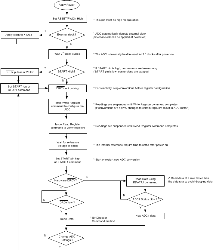
Figure 10-16 is a general procedure that shows a typical ADS1262 configuration and measurement sequence.
 Figure 10-16 ADS1262 Configuration and Measurement Procedure
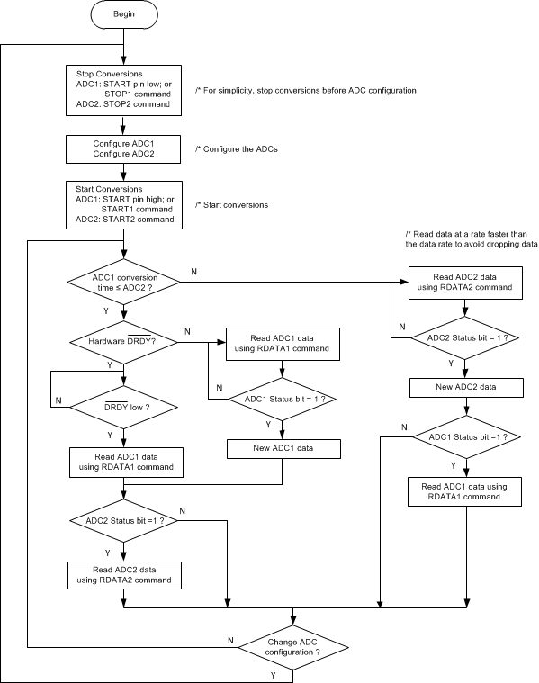
Figure 10-17 shows a general procedure to read concurrent ADC1 and ADC2 data of the ADS1263. The conversion time of ADC1 can be faster or slower than ADC2. If the conversion time of ADC1 is less than or equal to that of ADC2, and if the ADC2 status bit is equal to 1, then when ADC1 data are ready, ADC2 data are also ready. The ADC2 data can then be read by the RDATA2 command. Similarly, if the conversion time of ADC2 is less than that of ADC1, and if the ADC1 status bit is equal to 1, then when ADC2 data are ready. ADC1 data are also ready, The ADC1 data can then be read by the RDATA1 command. It is important to note an exception to the conversion time related to the data rate: the time of the first conversion is not always the same as (1 / data rate) because of digital filter latency. Therefore, it is possible that although the data rate of ADC1 can be faster than ADC2, the time required for the first conversion of ADC1 can be greater than ADC2 depending on the digital filter setting and chop mode. When checking the ADC2 status by reading ADC1 data, use the RDATA1 command.
 Figure 10-17 ADS1263 Concurrent Read of ADC1 and ADC2 Data