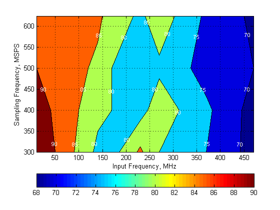
The ADS54J42 is a low-power, wide-bandwidth, 14-bit, 625-MSPS, dual-channel, analog-to-digital converter (ADC). Designed for high signal-to-noise ratio (SNR), the device delivers a noise floor of –157 dBFS/Hz for applications aiming for highest dynamic range over a wide instantaneous bandwidth. The device supports the JESD204B serial interface with data rates up to 6.25 Gbps. The buffered analog input provides uniform input impedance across a wide frequency range and minimizes sample-and-hold glitch energy. Each ADC channel optionally can be connected to a wideband digital down-converter (DDC) block. The ADS54J42 provides excellent spurious-free dynamic range (SFDR) over a large input frequency range with very low power consumption.
The JESD204B interface reduces the number of interface lines, allowing high system integration density. An internal phase-locked loop (PLL) multiplies the ADC sampling clock to derive the bit clock that is used to serialize the 14-bit data from each channel.
PART NUMBER | PACKAGE | BODY SIZE (NOM) |
---|---|---|
ADS54J42 | VQFNP (72) | 10.00 mm × 10.00 mm |
Changes from * Revision (February 2016) to A Revision
PIN | I/O | DESCRIPTION | |
---|---|---|---|
NAME | NO. | ||
CLOCK, SYSREF | |||
CLKINM | 28 | I | Negative differential clock input for the ADC |
CLKINP | 27 | I | Positive differential clock input for the ADC |
SYSREFM | 34 | I | Negative external SYSREF input |
SYSREFP | 33 | I | Positive external SYSREF input |
CONTROL, SERIAL | |||
PDN | 50 | I/O | Power-down. Can be configured via an SPI register setting. Can be configured to fast overrange output for channel A via the SPI. |
RESET | 48 | I | Hardware reset; active high. This pin has an internal 20-kΩ pulldown resistor. |
SCLK | 6 | I | Serial interface clock input |
SDIN | 5 | I | Serial interface data input |
SDOUT | 11 | O | Serial interface data output. Can be configured to fast overrange output for channel B via the SPI. |
SEN | 7 | I | Serial interface enable |
DATA INTERFACE | |||
DA0M | 62 | O | JESD204B serial data negative outputs for channel A |
DA1M | 59 | ||
DA2M | 56 | ||
DA3M | 54 | ||
DA0P | 61 | O | JESD204B serial data positive outputs for channel A |
DA1P | 58 | ||
DA2P | 55 | ||
DA3P | 53 | ||
DB0M | 65 | O | JESD204B serial data negative outputs for channel B |
DB1M | 68 | ||
DB2M | 71 | ||
DB3M | 1 | ||
DB0P | 66 | O | JESD204B serial data positive outputs for channel B |
DB1P | 69 | ||
DB2P | 72 | ||
DB3P | 2 | ||
SYNC | 63 | I | Synchronization input for the JESD204B port |
INPUT, COMMON MODE | |||
INAM | 41 | I | Differential analog negative input for channel A |
INAP | 42 | I | Differential analog positive input for channel A |
INBM | 14 | I | Differential analog negative input for channel B |
INBP | 13 | I | Differential analog positive input for channel B |
VCM | 22 | O | Common-mode voltage, 2.1 V. Note that analog inputs are internally biased to this pin through 600 Ω (effective), no external connection from the VCM pin to the INxP or INxM pin is required. |
POWER SUPPLY | |||
AGND | 18, 23, 26, 29, 32, 36, 37 | I | Analog ground |
AVDD | 9, 12, 15, 17, 25, 30, 35, 38, 40, 43, 44, 46 | I | Analog 1.9-V power supply |
AVDD3V | 10, 16, 24, 31, 39, 45 | I | Analog 3.0-V power supply for the analog buffer |
DGND | 3, 52, 60, 67 | I | Digital ground |
DVDD | 8, 47 | I | Digital 1.9-V power supply |
IOVDD | 4, 51, 57, 64, 70 | I | Digital 1.15-V power supply for the JESD204B transmitter |
NC, RES | |||
NC | 19-21 | — | Unused pins, do not connect |
RES | 49 | I | Reserved pin. Connect to DGND. |
MIN | MAX | UNIT | ||
---|---|---|---|---|
Supply voltage range | AVDD3V | –0.3 | 3.6 | V |
AVDD | –0.3 | 2.1 | ||
DVDD | –0.3 | 2.1 | ||
IOVDD | –0.2 | 1.4 | ||
Voltage between AGND and DGND | –0.3 | 0.3 | V | |
Voltage applied to input pins | INAP, INBP, INAM, INBM | –0.3 | 3 | V |
CLKINP, CLKINM | –0.3 | AVDD + 0.3 | ||
SYSREFP, SYSREFM | –0.3 | AVDD + 0.3 | ||
SCLK, SEN, SDIN, RESET, SYNC, PDN | –0.2 | 2.1 | ||
Storage temperature, Tstg | –65 | 150 | °C |
VALUE | UNIT | |||
---|---|---|---|---|
V(ESD) | Electrostatic discharge | Human-body model (HBM), per ANSI/ESDA/JEDEC JS-001(1) | ±1000 | V |
Charged-device model (CDM), per JEDEC specification JESD22-C101(2) | ±500 |
MIN | NOM | MAX | UNIT | |||
---|---|---|---|---|---|---|
Supply voltage range | AVDD3V | 2.85 | 3.0 | 3.6 | V | |
AVDD | 1.8 | 1.9 | 2.0 | |||
DVDD | 1.7 | 1.9 | 2.0 | |||
IOVDD | 1.1 | 1.15 | 1.2 | |||
Analog inputs | Differential input voltage range | 1.9 | VPP | |||
Input common-mode voltage | 2.0 | V | ||||
Maximum analog input frequency for a 1.9-VPP input amplitude(4)(5) | 400 | MHz | ||||
Clock inputs | Input clock frequency, device clock frequency | 300(6) | 625 | MHz | ||
Input clock amplitude differential (VCLKP – VCLKM) |
Sine wave, ac-coupled | 0.75 | 1.5 | VPP | ||
LVPECL, ac-coupled | 0.8 | 1.6 | ||||
LVDS, ac-coupled | 0.7 | |||||
Input device clock duty cycle | 45% | 50% | 55% | |||
Temperature | Operating free-air, TA | –40 | 85 | ºC | ||
Operating junction, TJ | 105(1) | 125 |
THERMAL METRIC(1) | ADS54J42 | UNIT | |
---|---|---|---|
RMP (VQFNP) | |||
72 PINS | |||
RθJA | Junction-to-ambient thermal resistance | 22.3 | °C/W |
RθJC(top) | Junction-to-case (top) thermal resistance | 5.1 | °C/W |
RθJB | Junction-to-board thermal resistance | 2.4 | °C/W |
ψJT | Junction-to-top characterization parameter | 0.1 | °C/W |
ψJB | Junction-to-board characterization parameter | 2.3 | °C/W |
RθJC(bot) | Junction-to-case (bottom) thermal resistance | 0.4 | °C/W |
PARAMETER | TEST CONDITIONS | MIN | TYP | MAX | UNIT | ||
---|---|---|---|---|---|---|---|
GENERAL | |||||||
ADC sampling rate | 625 | MSPS | |||||
Resolution | 14 | Bits | |||||
POWER SUPPLIES | |||||||
AVDD3V | 3.0-V analog supply | 2.85 | 3.0 | 3.6 | V | ||
AVDD | 1.9-V analog supply | 1.8 | 1.9 | 2.0 | V | ||
DVDD | 1.9-V digital supply | 1.7 | 1.9 | 2.0 | V | ||
IOVDD | 1.15-V SERDES supply | 1.1 | 1.15 | 1.2 | V | ||
IAVDD3V | 3.0-V analog supply current | VIN = full-scale on both channels | 247 | 310 | mA | ||
IAVDD | 1.9-V analog supply current | VIN = full-scale on both channels | 260 | 410 | mA | ||
IDVDD | 1.9-V digital supply current | Eight lanes active (LMFS = 8224) |
137 | 210 | mA | ||
IIOVDD | 1.15-V SERDES supply current | Eight lanes active (LMFS = 8224) |
382 | 720 | mA | ||
Pdis | Total power dissipation | Eight lanes active (LMFS = 8224) |
1.94 | 2.68 | W | ||
IDVDD | 1.9-V digital supply current | Four lanes active (LMFS = 4222), 2X decimation | 130 | mA | |||
IIOVDD | 1.15-V SERDES supply current | Four lanes active (LMFS = 4222), 2X decimation | 404 | mA | |||
Pdis | Total power dissipation | Four lanes active (LMFS = 4222), 2X decimation | 1.95 | W | |||
IDVDD | 1.9-V digital supply current | Two lanes active (LMFS = 2221), 4X decimation | 129 | mA | |||
IIOVDD | 1.15-V SERDES supply current | Two lanes active (LMFS = 2221), 4X decimation | 400 | mA | |||
Pdis(1) | Total power dissipation | Two lanes active (LMFS = 2221), 4X decimation | 1.94 | W | |||
Global power-down power dissipation | 285 | 315 | mW | ||||
ANALOG INPUTS (INAP, INAM, INBP, INBM) | |||||||
Differential input full-scale voltage | 1.9 | VPP | |||||
VIC | Common-mode input voltage | 2.0 | V | ||||
RIN | Differential input resistance | At 170-MHz input frequency | 0.6 | kΩ | |||
CIN | Differential input capacitance | At 170-MHz input frequency | 4.7 | pF | |||
Analog input bandwidth (3 dB) | 50-Ω source driving ADC inputs terminated with 50 Ω | 1.2 | GHz | ||||
CLOCK INPUT (CLKINP, CLKINM) | |||||||
Internal clock biasing | CLKINP and CLKINM are connected to internal biasing voltage through 400 Ω | 1.15 | V |
PARAMETER | TEST CONDITIONS | MIN | TYP | MAX | UNITS | |
---|---|---|---|---|---|---|
DIGITAL INPUTS (RESET, SCLK, SEN, SDIN, SYNC, PDN)(1) | ||||||
VIH | High-level input voltage | All digital inputs support 1.2-V and 1.8-V logic levels | 0.8 | V | ||
VIL | Low-level input voltage | All digital inputs support 1.2-V and 1.8-V logic levels | 0.4 | V | ||
IIH | High-level input current | SEN | 0 | µA | ||
RESET, SCLK, SDIN, PDN, SYNC | 50 | |||||
IIL | Low-level input current | SEN | 50 | µA | ||
RESET, SCLK, SDIN, PDN, SYNC | 0 | |||||
DIGITAL INPUTS (SYSREFP, SYSREFM) | ||||||
VD | Differential input voltage | 0.35 | 0.45 | 1.4 | V | |
V(CM_DIG) | Common-mode voltage for SYSREF(3) | 1.3 | V | |||
DIGITAL OUTPUTS (SDOUT, PDN(3)) | ||||||
VOH | High-level output voltage | DVDD – 0.1 | DVDD | V | ||
VOL | Low-level output voltage | 0.1 | V | |||
DIGITAL OUTPUTS (JESD204B Interface: DxP, DxM)(2) | ||||||
VOD | Output differential voltage | With default swing setting | 700 | mVPP | ||
VOC | Output common-mode voltage | 450 | mV | |||
Transmitter short-circuit current | Transmitter pins shorted to any voltage between –0.25 V and 1.45 V | –100 | 100 | mA | ||
zos | Single-ended output impedance | 50 | Ω | |||
Output capacitance | Output capacitance inside the device, from either output to ground |
2 | pF |
MIN | TYP | MAX | UNITS | |||
---|---|---|---|---|---|---|
SAMPLE TIMING | ||||||
Aperture delay | 0.75 | 1.6 | ns | |||
Aperture delay matching between two channels on the same device | ±70 | ps | ||||
Aperture delay matching between two devices at the same temperature and supply voltage | ±270 | ps | ||||
Aperture jitter | 120 | fS rms | ||||
WAKE-UP TIMING | ||||||
Wake-up time to valid data after coming out of global power-down | 150 | µs | ||||
LATENCY | ||||||
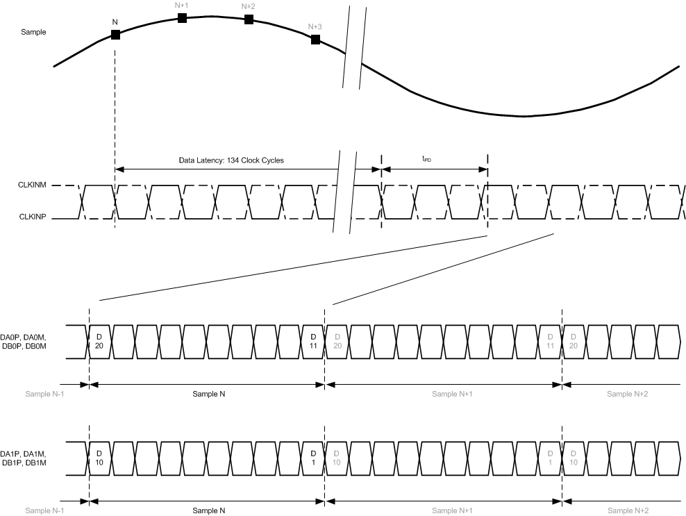
Data latency(1): ADC sample to digital output | 134 | Input clock cycles | ||||
OVR latency: ADC sample to OVR bit | 62 | Input clock cycles | ||||
tPD | Propagation delay: logic gates and output buffers delay (does not change with fS) | 4 | ns | |||
SYSREF TIMING | ||||||
tSU_SYSREF | Setup time for SYSREF, referenced to the input clock falling edge | 300 | 900 | ps | ||
tH_SYSREF | Hold time for SYSREF, referenced to the input clock falling edge | 100 | ps | |||
JESD OUTPUT INTERFACE TIMING CHARACTERISTICS | ||||||
Unit interval | 160 | 400 | ps | |||
Serial output data rate | 2.5 | 6.25 | Gbps | |||
Total jitter for BER of 1E-15 and lane rate = 6.25 Gbps | 26 | ps | ||||
Random jitter for BER of 1E-15 and lane rate = 6.25 Gbps | 0.75 | ps rms | ||||
Deterministic jitter for BER of 1E-15 and lane rate = 6.25 Gbps | 12 | ps, pk-pk | ||||
tR, tF | Data rise time, data fall time: rise and fall times are measured from 20% to 80%, differential output waveform, 2.5 Gbps ≤ bit rate ≤ 6.25 Gbps |
35 | ps |
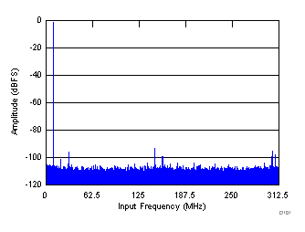
SNR = 71.9 dBFS, SINAD = 71.86 dBFS, THD = 93 dBc, IL spur = 94 dBc, SFDR = 94 dBc, non HD2, HD3 spur = 94 dBc |
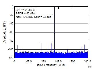
SNR = 71 dBFS, SINAD = 70.9 dBFS, SFDR = 85 dBc, THD = 84 dBc, IL spur = 87 dBc, non HD2, HD3 spur = 93 dBc |
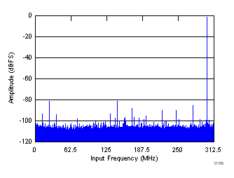
SNR = 69.5 dBFS, SINAD = 69.1 dBFS, IL spur = 81 dBc, SFDR = 80 dBc, THD = 79 dBc, non HD2, HD3 spur = 90 dBc |
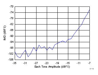
fIN1 = 185 MHz, fIN2 = 190 MHz, each tone at –36 dBFS, IMD = 107 dBFS |
fIN1 = 370 MHz, fIN2 = 365 MHz, each tone at –36 dBFS, IMD = 109 dBFS |
fIN1 = 470 MHz, fIN2 = 465 MHz, each tone at –36 dBFS, IMD = 107 dBFS |
fIN1 = 365 MHz, fIN2 = 370 MHz |
fIN = 170 MHz |
fIN = 350 MHz |
fIN = 170 MHz |
fIN = 350 MHz |
fIN = 170 MHz |
fIN = 350 MHz |
fIN = 350 MHz |
fIN = 350 MHz |
fIN = 350 MHz |
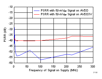
fIN = 170 MHz, AIN = –1 dBFS, fPSRR = 5 MHz, APSRR= 50 mVPP, PSRR (AVDD supply) = 51 dB |
fIN = 170 MHz, AIN = –1 dBFS, fCMRR = 5 MHz, ACMRR= 50 mVPP, CMRR = 40 dB |
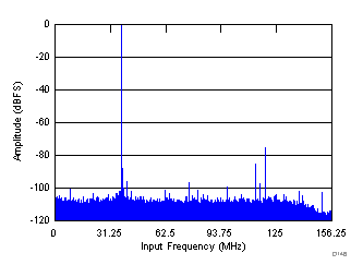
SNR = 72 dBFS, SINAD = 71.8 dBFS, SFDR = 84 dBc, THD = 83 dBc, non HD2, HD3 spur = 98 dBc |
SNR = 77.4 dBFS, SINAD = 77.3 dBFS, SFDR = 105 dBc, THD = 102 dBc, non HD2, HD3 spur = 105 dBc |
SNR = 74.9 dBFS, SINAD = 74.8 dBFS, SFDR = 93 dBc, THD = 92 dBc, non HD2, HD3 spur = 93 dBc |
SNR = 71.3 dBFS, SINAD = 71.1 dBFS, SFDR = 86 dBc, THD = 85 dBc, IL spur = 87 dBc, non HD2, HD3 spur = 95 dBc |
SNR = 70.4 dBFS, SINAD = 69.9 dBFS, IL spur = 89 dBc, SFDR = 80 dBc, THD = 79 dBc, non HD2, HD3 spur = 91 dBc |
SNR = 68.8 dBFS, SINAD = 67.3 dBFS, SFDR = 73 dBc, THD = 72 dBc, IL spur = 81 dBc, non HD2, HD3 spur = 89 dBc |
fIN1 = 185 MHz, fIN2 = 190 MHz, each tone at –7 dBFS, IMD = 89 dBFS |
||
fIN1 = 370 MHz, fIN2 = 365 MHz, each tone at –7 dBFS, IMD = 78 dBFS |
fIN1 = 470 MHz, fIN2 = 465 MHz, each tone at –7 dBFS, IMD = 71 dBFS |
fIN1 = 185 MHz, fIN2 = 190 MHz | ||
fIN1 = 465 MHz, fIN2 = 470 MHz |
fIN = 170 MHz |
fIN = 350 MHz |
fIN = 170 MHz |
fIN = 350 MHz |
fIN = 170 MHz |
fIN = 350 MHz |
fIN = 170 MHz |
fIN = 170 MHz |
fIN = 170 MHz |
NOTE: ADC output amplitude is –1 dBFS, input amplitude is scaled down by the amount of programmed digital gain. |
SNR = 74.1 dBFS, SINAD = 74.09 dBFS, SFDR = 98 dBc, THD = 93 dBc, non HD2, HD3 spur = 99 dBc |
SNR = 77.6 dBFS, SINAD = 77.5 dBFS, SFDR = 93 dBc, THD = 92 dBc, non HD2, HD3 spur = 106 dBc |
SNR = 76.7 dBFS, SINAD = 76.6 dBFS, SFDR = 96 dBc, THD = 98 dBc, non HD2, HD3 spur = 96 dBc |
The ADS54J42 is a low-power, wide-bandwidth, 14-bit, 625-MSPS, dual-channel, analog-to-digital converter (ADC). The ADS54J42 employs four interleaving ADCs for each channel to achieve a noise floor of –157 dBFS/Hz. The ADS54J42 uses TI's proprietary interleaving and dither algorithms to achieve a clean spectrum with a high spurious-free dynamic range (SFDR). The device also offers various programmable decimation filtering options for systems requiring higher signal-to-noise ratio (SNR) and SFDR over a wide range of frequencies.
Analog input buffers isolate the ADC driver from glitch energy generated from sampling process, thereby simplify the driving network on-board. The JESD204B interface reduces the number of interface lines with two-lane and four-lane options, allowing a high system integration density. The JESD204B interface operates in subclass 1, enabling multi-chip synchronization with the SYSREF input.
The ADS54J42 analog signal inputs are designed to be driven differentially. The analog input pins have internal analog buffers that drive the sampling circuit. As a result of the analog buffer, the input pins present a high impedance input across a very wide frequency range to the external driving source that enables great flexibility in the external analog filter design as well as excellent 50-Ω matching for RF applications. The buffer also helps isolate the external driving circuit from the internal switching currents of the sampling circuit, resulting in a more constant SFDR performance across input frequencies.
The common-mode voltage of the signal inputs is internally biased to VCM using 600-Ω resistors, allowing for ac-coupling of the input drive network. Each input pin (INP, INM) must swing symmetrically between (VCM + 0.475 V) and (VCM – 0.475 V), resulting in a 1.9-VPP (default) differential input swing. The input sampling circuit has a 3-dB bandwidth that extends up to 1.2 GHz. An equivalent analog input network diagram is shown in Figure 58.
The input bandwidth shown in Figure 59 is measured with respect to a 50-Ω differential input termination at the ADC input pins.
The ADS54J42 has an optional DDC block that can be enabled via an SPI register write. Each ADC channel is followed by a DDC block consisting of three different decimate-by-2 and decimate-by-4 finite impulse response (FIR) half-band filter options. The different decimation filter options can be selected via SPI programming.
Figure 60 shows the signal processing done inside the DDC block of the ADS54J42.
This decimation filter has 41 taps. The stop-band attenuation is approximately 90 dB and the pass-band flatness is ±0.05 dB. Table 1 shows corner frequencies for the low-pass and high-pass filter options.
CORNERS (dB) | LOW PASS | HIGH PASS |
---|---|---|
–0.1 | 0.202 × fS | 0.298 × fS |
–0.5 | 0.210 × fS | 0.290 × fS |
–1 | 0.215 × fS | 0.285 × fS |
–3 | 0.227 × fS | 0.273 × fS |
Figure 61 and Figure 62 show the frequency response of the decimate-by-2 filter from dc to fS / 2.
This band-pass decimation filter consists of a digital mixer and three concatenated FIR filters with a combined latency of approximately 28 output clock cycles. The alias band attenuation is approximately 55 dB and the pass-band flatness is ±0.1 dB. By default after reset, the band-pass filter is centered at fS / 16. Using the SPI, the center frequency can be programmed at N × fS / 16 (where N = 1, 3, 5, or 7). Table 2 shows corner frequencies for two extreme options.
CORNERS (dB) | CORNER FREQUENCY AT LOWER SIDE (Center Frequency fS / 16) | CORNER FREQUENCY AT HIGHER SIDE (Center Frequency fS / 16) |
---|---|---|
–0.1 | 0.011 × fS | 0.114 × fS |
–0.5 | 0.010 × fS | 0.116 × fS |
–1 | 0.008 × fS | 0.117 × fS |
–3 | 0.006 × fS | 0.120 × fS |
Figure 63 and Figure 64 show the frequency response of the decimate-by-4 filter for center frequencies fS / 16 and 3 × fS / 16 (N = 1 and N = 3, respectively).
In this configuration, the DDC block includes a fixed digital fS / 4 mixer. Thus, the IQ pass band is approximately ±0.11 fS, centered at fS / 4. This decimation filter has 41 taps with a latency of approximately ten output clock cycles. The stop-band attenuation is approximately 90 dB and the pass-band flatness is ±0.05 dB. Table 3 shows the corner frequencies for a low-pass, decimate-by-4 IQ filter.
CORNERS (dB) | LOW PASS |
---|---|
–0.1 | 0.107 × fS |
–0.5 | 0.112 × fS |
–1 | 0.115 × fS |
–3 | 0.120 × fS |
Figure 65 and Figure 66 show the frequency response of a decimate-by-4 IQ output filter from dc to fS / 2.
The SYSREF signal is a periodic signal that is sampled by the ADS54J42 device clock and used to align the boundary of the local multi-frame clock inside the data converter. SYSREF is required to be a sub-harmonic of the local multiframe clock (LMFC) internal timing. To meet this requirement, the timing of SYSREF is dependent on the device clock frequency and the LMFC frequency, as determined by the selected DDC decimation and frames per multi-frame settings. The SYSREF signal is recommended to be a low-frequency signal in the range of 1 MHz to 5 MHz to reduce coupling to the signal path both on the printed circuit board (PCB) as well as internal to the device.
The external SYSREF signal must be a sub-harmonic of the internal LMFC clock, as shown in Equation 1 and Table 4.
where
LMFS CONFIGURATION | DECIMATION | LMFC CLOCK(1)(2) |
---|---|---|
4211 | — | fS / K |
4244 | — | (fS / 4) / K |
8224 | — | (fS / 4) / K |
4222 | 2X | (fS / 4) / K |
2242 | 2X | (fS / 4) / K |
2221 | 4X | (fS / 4) / K |
2441 | 4X (IQ) | (fS / 4) / K |
4421 | 4X (IQ) | (fS / 4) / K |
1241 | 4X | (fS / 4) / K |
For example, if LMFS = 8224, the default value of K is 8 + 1 = 9 (the actual value for K = the value set in the SPI register + 1). If the device clock frequency is fS = 625 MSPS, then the local multi-frame clock frequency becomes (625 / 4) / 9 = 17.361111 MHz. The SYSREF signal frequency can be chosen as LMFC frequency / 8 = 2.1701389 MHz.
The ADS54J42 provides a fast overrange indication that can be presented in the digital output data stream via SPI configuration. Alternatively, if not used, the SDOUT (pin 11) and PDN (pin 50) pins can be configured via the SPI to output the fast OVR indicator.
The JESD 8b, 10b encoder receives 16-bit data that is formed by 14-bit ADC data padded with two 0s as LSBs. When the FOVR indication is embedded in the output data stream, the LSB of the 16-bit data stream going to the 8b, 10b encoder is replaced, as shown in Figure 67.
The fast OVR is triggered if the input voltage exceeds the programmable overrange threshold and is presented after only seven clock cycles, thus enabling a quicker reaction to an overrange event.
The input voltage level that the overload is detected at is referred to as the threshold. The threshold is programmable using the FOVR THRESHOLD bits, as shown in Figure 68. The FOVR is triggered seven output clock cycles after the overload condition occurs.
The input voltage level that the fast OVR is triggered at is defined by Equation 2:
The default threshold is E3h (227d), corresponding to a threshold of –1 dBFS.
In terms of full-scale input, the fast OVR threshold can be calculated as Equation 3:
The ADS54J42 provides a highly-configurable power-down mode. Power-down can be enabled using the PDN pin or SPI register writes.
A power-down mask can be configured that allows a trade-off between wake-up time and power consumption in power-down mode. Two independent power-down masks can be configured: MASK 1 and MASK 2, as shown in Table 5. See the master page registers in Table 14 for further details.
REGISTER ADDRESS | COMMENT | REGISTER DATA | |||||||
---|---|---|---|---|---|---|---|---|---|
A[7:0] (Hex) | 7 | 6 | 5 | 4 | 3 | 2 | 1 | 0 | |
MASTER PAGE (80h) | |||||||||
20 | MASK 1 | PDN ADC CHA | PDN ADC CHB | ||||||
21 | PDN BUFFER CHB | PDN BUFFER CHA | 0 | 0 | 0 | 0 | |||
23 | MASK 2 | PDN ADC CHA | PDN ADC CHB | ||||||
24 | PDN BUFFER CHB | PDN BUFFER CHA | 0 | 0 | 0 | 0 | |||
26 | CONFIG | GLOBAL PDN | OVERRIDE PDN PIN | PDN MASK SEL | 0 | 0 | 0 | 0 | 0 |
53 | 0 | MASK SYSREF | 0 | 0 | 0 | 0 | 0 | 0 | |
55 | 0 | 0 | 0 | PDN MASK | 0 | 0 | 0 | 0 |
To save power, the device can be put in complete power-down by using the GLOBAL PDN register bit. However, when JESD is required to remain active when putting the device in power-down, the ADC and analog buffer can be powered down by using the PDN ADC CHx and PDN BUFFER CHx register bits after enabling the PDN MASK register bit. The PDN MASK SEL register bit can be used to select between MASK 1 or MASK 2. Table 6 shows the power consumption for different combinations of the GLOBAL PDN, PDN ADC CHx, and PDN BUFF CHx register bits.
REGISTER BIT | COMMENT | IAVDD3V (mA) | IAVDD (mA) | IDVDD (mA) | IIOVDD (mA) | TOTAL POWER (W) |
---|---|---|---|---|---|---|
Default | After reset, with a full-scale input signal to both channels | 247 | 260 | 137 | 382 | 1.94 |
GBL PDN = 1 | The device is in a complete power-down state | 3 | 6 | 23 | 192 | 0.28 |
GBL PDN = 0, PDN ADC CHx = 1 (x = A or B) |
The ADC of one channel is powered down | 206 | 166 | 97 | 367 | 1.54 |
GBL PDN = 0, PDN BUFF CHx = 1 (x = A or B) |
The input buffer of one channel is powered down | 195 | 258 | 137 | 381 | 1.78 |
GBL PDN = 0, PDN ADC CHx = 1, PDN BUFF CHx = 1 (x = A or B) |
The ADC and input buffer of one channel are powered down | 152 | 166 | 97 | 363 | 1.37 |
GBL PDN = 0, PDN ADC CHx = 1, PDN BUFF CHx = 1 (x = A and B) |
The ADC and input buffer of both channels are powered down | 55 | 70 | 56 | 356 | 0.81 |
The ADS54J42 can be configured by using a serial programming interface, as described in the Serial Interface section. In addition, the device has one dedicated parallel pin (PDN) for controlling the power-down mode.
The ADS54J42 supports a 24-bit (16-bit address, 8-bit data) SPI operation and uses paging (see the Register Maps section) to access all register bits.
The ADC has a set of internal registers that can be accessed by the serial interface formed by the SEN (serial interface enable), SCLK (serial interface clock), and SDIN (serial interface data) pins, as shown in Figure 69. SPI bits in Figure 69 are explained in Table 7. Serially shifting bits into the device is enabled when SEN is low. Serial data on SDIN are latched at every SCLK rising edge when SEN is active (low). The interface can function with SCLK frequencies from 2 MHz down to very low speeds (of a few hertz) and also with a non-50% SCLK duty cycle.
SPI BITS | DESCRIPTION | BIT SETTINGS |
---|---|---|
R/W | Read/write bit | 0 = SPI write 1 = SPI read back |
M | SPI bank access | 0 = Analog SPI bank (master and ADC pages) 1 = JESD SPI bank (main digital, JESD analog, and JESD digital pages) |
P | JESD page selection bit | 0 = Page access 1 = Register access |
CH | SPI access for a specific channel of the JESD SPI bank | 0 = Channel A 1 = Channel B By default, both channels are being addressed. |
A[11:0] | SPI address bits | — |
D[7:0] | SPI data bits | — |
Table 8 shows the timing requirements for the serial interface signals in Figure 69.
MIN | TYP | MAX | UNIT | ||
---|---|---|---|---|---|
fSCLK | SCLK frequency (equal to 1 / tSCLK) | > dc | 2 | MHz | |
tSLOADS | SEN to SCLK setup time | 100 | ns | ||
tSLOADH | SCLK to SEN hold time | 100 | ns | ||
tDSU | SDIN setup time | 100 | ns | ||
tDH | SDIN hold time | 100 | ns |
The analog SPI bank contains two pages (the master and ADC pages). The internal register of the ADS54J42 analog SPI bank can be programmed by:
The content from one of the two analog banks can be read out by:
The JESD SPI bank contains four pages (main digital, JESD digital, and JESD analog pages). The individual pages can be selected by:
The ADS54J42 is a dual-channel device and the JESD204B portion is configured individually for each channel by using the CH bit. Note that the P bit must be set to 1 for register writes.
By default, register writes are applied to both channels. To enable individual channel writes, write address 4005h with 01h (default is 00h).
The content from one of the pages of the JESD bank can be read out by:
The ADS54J42 supports device subclass 1 with a maximum output data rate of 6.25 Gbps for each serial transmitter.
An external SYSREF signal is used to align all internal clock phases and the local multi-frame clock to a specific sampling clock edge, allowing synchronization of multiple devices in a system and minimizing timing and alignment uncertainty. The SYNC input is used to control the JESD204B SERDES blocks.
Depending on the ADC output data rate, the JESD204B output interface can be operated with either two or four lanes per single ADC, as shown in Figure 75. The JESD204B setup and configuration of the frame assembly parameters is controlled via the SPI interface.
The JESD204B transmitter block shown in Figure 76 consists of the transport layer, the data scrambler, and the link layer. The transport layer maps the ADC output data into the selected JESD204B frame data format. The link layer performs the 8b, 10b data encoding as well as the synchronization and initial lane alignment using the SYNC input signal. Optionally, data from the transport layer can be scrambled.
The initial lane alignment process is started when the receiving device de-asserts the SYNC signal, as shown in Figure 77. When a logic low is detected on the SYNC input pin, the ADS54J42 starts transmitting comma (K28.5) characters to establish a code group synchronization.
When synchronization is complete, the receiving device asserts the SYNC signal and the ADS54J42 starts the initial lane alignment sequence with the next local multi-frame clock boundary. The ADS54J42 transmits four multi-frames, each containing K frames (K is SPI programmable). Each of the multi-frames contains the frame start and end symbols and the second multi-frame also contains the JESD204 link configuration data.
There are three different test patterns available in the transport layer of the JESD204B interface. The ADS54J42 supports a clock output, encoded, and a PRBS (215 – 1) pattern. These test patterns can be enabled via an SPI register write and are located in the JESD digital page of the JESD bank.
The JESD204B standard defines the following parameters:
Table 9 lists the available JESD204B formats and valid ranges for the ADS54J42 when the decimation filter is not used. The ranges are limited by the SERDES lane rate and the maximum ADC sample frequency.
NOTE
The 16-bit data going to the JESD 8b, 10b encoder is formed by padding two 0s as LSBs into the 14-bit ADC data.
L | M | F | S | DECIMATION | MINIMUM RATES | MAXIMUM RATES | ||
---|---|---|---|---|---|---|---|---|
SAMPLING RATE (MSPS) | SERDES BIT RATE (Gbps) | SAMPLING RATE (MSPS) | SERDES BIT RATE (Gbps) | |||||
4 | 2 | 1 | 1 | Not used | 250 | 2.5 | 625 | 6.25 |
4 | 2 | 4 | 4 | Not used | 250 | 2.5 | 625 | 6.25 |
8 | 2 | 2 | 4 | Not used | 500 | 2.5 | 625 | 3.125 |
NOTE
In the LMFS = 8224 row of Table 9, the sample order in lane DA2 and DA3 are swapped.
The detailed frame assembly is shown in Table 10.
PIN | LMFS = 4211 | LMFS = 4244 | LMFS = 8224 | ||||
---|---|---|---|---|---|---|---|
DA0 | A3[15:8] | A3[7:0] | |||||
DA1 | A0[7:0] | A2[15:8] | A2[7:0] | A3[15:8] | A3[7:0] | A2[15:8] | A2[7:0] |
DA2 | A0[15:8] | A0[15:8] | A0[7:0] | A1[15:8] | A1[7:0] | A0[15:8] | A0[7:0] |
DA3 | A1[15:8] | A1[7:0] | |||||
DB0 | B3[15:8] | B3[7:0] | |||||
DB1 | B0[7:0] | B2[15:8] | B2[7:0] | B3[15:8] | B3[7:0] | B2[15:8] | B2[7:0] |
DB2 | B0[15:8] | B0[15:8] | B0[7:0] | B1[15:8] | B1[7:0] | B0[15:8] | B0[7:0] |
DB3 | B1[15:8] | B1[7:0] |
Table 11 lists the available JESD204B formats and valid ranges for the ADS54J42 when enabling the decimation filter. The ranges are limited by the SERDES lane rate (2.5 Gbps to 6.25 Gbps) and the ADC sample frequency (300 MSPS to 625 MSPS).
L | M | F | S | DECIMATION | MINIMUM RATES | MAXIMUM RATES | ||||
---|---|---|---|---|---|---|---|---|---|---|
DEVICE CLOCK FREQUENCY (MSPS) | OUTPUT SAMPLE RATE (MSPS) | SERDES BIT RATE (Gbps) | DEVICE CLOCK FREQUENCY (MSPS) | OUTPUT SAMPLE RATE (MSPS) | SERDES BIT RATE (Gbps) | |||||
4 | 4 | 2 | 1 | 4X (IQ) | 500 | 125 | 2.5 | 625 | 156.25 | 3.125 |
4 | 2 | 2 | 2 | 2X | 500 | 250 | 2.5 | 625 | 312.5 | 3.125 |
2 | 2 | 4 | 2 | 2X | 300 | 150 | 3 | 625 | 312.5 | 6.25 |
2 | 2 | 2 | 1 | 4X | 500 | 125 | 2.5 | 625 | 156.25 | 3.125 |
2 | 4 | 4 | 1 | 4X (IQ) | 300 | 75 | 3 | 625 | 156.25 | 6.25 |
1 | 2 | 4 | 1 | 4X | 300 | 75 | 3 | 625 | 156.25 | 6.25 |
Table 12 lists the detailed frame assembly with different decimation options.
PIN | LMFS = 4222, 2X DECIMATION | LMFS = 2242, 2X DECIMATION | LMFS = 2221, 4X DECIMATION | LMFS = 2441, 4X DECIMATION (IQ) | LMFS = 4421, 4X DECIMATION (IQ) | LMFS = 1241, 4X DECIMATION | ||||||||||||
---|---|---|---|---|---|---|---|---|---|---|---|---|---|---|---|---|---|---|
DA0 | A1 [15:8] |
A1 [7:0] |
AQ0 [15:8] |
AQ0 [7:0] |
||||||||||||||
DA1 | A0 [15:8] |
A0 [7:0] |
A0 [15:8] |
A0 [7:0] |
A1 [15:8] |
A1 [7:0] |
A0 [15:8] |
A0 [7:0] |
AI0 [15:8] |
AI0 [7:0] |
AQ0 [15:8] |
AQ0 [7:0] |
AI0 [15:8] |
AI0 [7:0] |
A0 [15:8] |
A0 [7:0] |
B0 [15:8] |
B0 [7:0] |
DA2 | ||||||||||||||||||
DA3 | ||||||||||||||||||
DB0 | B1 [15:8] |
B1 [7:0] |
BQ0 [15:8] |
BQ0 [7:0] |
||||||||||||||
DB1 | B0 [15:8] |
B0 [7:0] |
B0 [15:8] |
B0 [7:0] |
B1 [15:8] |
B1 [7:0] |
B0 [15:8] |
B0 [7:0] |
BI0 [15:8] |
BI0 [7:0] |
BQ0 [15:8] |
BQ0 [7:0] |
BI0 [15:8] |
BI0 [7:0] |
||||
DB2 | ||||||||||||||||||
DB3 |
Appropriate register bits must be programmed to enable different options when the decimation filter is enabled. Table 13 summarizes all the decimation filter options available in the DDC block, the corresponding JESD link parameters (L, M, F, and S), and the register bits required to be programmed for each option.
LMFS OPTIONS | DDC MODES PROGRAMMING | JESD LINK (LMFS) PROGRAMMING | ||||||||||||
---|---|---|---|---|---|---|---|---|---|---|---|---|---|---|
L | M | F | S | DECIMATION OPTIONS | DEC MODE EN, DECFIL EN(3) | DECFIL MODE[3:0](4) | JESD FILTER(5) | JESD MODE(6) | JESD PLL MODE(7) | LANE SHARE(8) | DA_BUS_ REORDER(9) |
DB_BUS_ REORDER(10) |
BUS_REORDER EN1(11) | BUS_REORDER EN2(12) |
4 | 2 | 1 | 1 | No decimation | 00 | 00 | 000 | 100 | 10 | 0 | 00h | 00h | 0 | 0 |
4 | 2 | 4 | 4 | No decimation | 00 | 00 | 000 | 010 | 10 | 0 | 00h | 00h | 0 | 0 |
8 | 2 | 2 | 4 | No decimation (Default after reset) | 00 | 00 | 000 | 001 | 00 | 0 | 00h | 00h | 0 | 0 |
4 | 4 | 2 | 1 | 4X (IQ) | 11 | 0011 (LPF with fS / 4 mixer) | 111 | 001 | 00 | 0 | 0Ah | 0Ah | 1 | 1 |
4 | 2 | 2 | 2 | 2X | 11 | 0010 (LPF) or 0110 (HPF) | 110 | 001 | 00 | 0 | 0Ah | 0Ah | 1 | 1 |
2 | 2 | 4 | 2 | 2X | 11 | 0010 (LPF) or 0110 (HPF) | 110 | 010 | 10 | 0 | 0Ah | 0Ah | 1 | 1 |
2 | 2 | 2 | 1 | 4X | 11 | 0000, 0100, 1000, or 1100 (all BPFs with different center frequencies). | 100 | 001 | 00 | 0 | 0Ah | 0Ah | 1 | 1 |
2 | 4 | 4 | 1 | 4X (IQ) | 11 | 0011 (LPF with an fS / 4 mixer) | 111 | 010 | 10 | 0 | 0Ah | 0Ah | 1 | 1 |
1 | 2 | 4 | 1 | 4X | 11 | 0000, 0100, 1000, or 1100 (all BPFs with different center frequencies) | 100 | 010 | 10 | 1 | 0Ah | 0Ah | 1 | 1 |
Each of the 6.25-Gbps SERDES JESD transmitter outputs requires ac-coupling between the transmitter and receiver. The differential pair must be terminated with 100-Ω resistors as close to the receiving device as possible to avoid unwanted reflections and signal degradation, as shown in Figure 78.
Figure 79 and Figure 80 show the serial output eye diagrams of the ADS54J42 at 6.25 Gbps and 2.5 Gbps (respectively) with default output voltage swings against the JESD204B mask.
Figure 81 shows a conceptual diagram of the serial registers.
The ADS54J42 contains two main SPI banks. The analog SPI bank provides access to the ADC analog blocks and the digital SPI bank controls the interleaving engine and anything related to the JESD204B serial interface. The analog SPI bank is divided into two pages (master and ADC) and the digital SPI bank is divided into three pages (main digital, JESD digital, and JESD analog). Table 14 lists a register map for the ADS54J42.
REGISTER ADDRESS | REGISTER DATA | |||||||
---|---|---|---|---|---|---|---|---|
A[11:0] (Hex) | 7 | 6 | 5 | 4 | 3 | 2 | 1 | 0 |
GENERAL REGISTERS | ||||||||
0 | RESET | 0 | 0 | 0 | 0 | 0 | 0 | RESET |
3 | JESD BANK PAGE SEL[7:0] | |||||||
4 | JESD BANK PAGE SEL[15:8] | |||||||
5 | 0 | 0 | 0 | 0 | 0 | 0 | 0 | DISABLE BROADCAST |
11 | ANALOG BANK PAGE SEL | |||||||
MASTER PAGE (80h) | ||||||||
20 | PDN ADC CHA | PDN ADC CHB | ||||||
21 | PDN BUFFER CHB | PDN BUFFER CHA | 0 | 0 | 0 | 0 | ||
23 | PDN ADC CHA | PDN ADC CHB | ||||||
24 | PDN BUFFER CHB | PDN BUFFER CHA | 0 | 0 | 0 | 0 | ||
26 | GLOBAL PDN | OVERRIDE PDN PIN | PDN MASK SEL | 0 | 0 | 0 | 0 | 0 |
39 | HIGH FREQ 1 | HIGH FREQ 0 | 0 | 0 | 0 | 0 | 0 | 0 |
3A | 0 | HIGH FREQ 2 | 0 | 0 | 0 | 0 | 0 | 0 |
4F | 0 | 0 | 0 | 0 | 0 | 0 | 0 | EN INPUT DC COUPLING |
53 | 0 | MASK SYSREF | 0 | 0 | 0 | 0 | EN SYSREF DC COUPLING | 0 |
55 | 0 | 0 | 0 | PDN MASK | 0 | 0 | 0 | 0 |
56 | 0 | 0 | 0 | 0 | 0 | HIGH FREQ 3 | 0 | 0 |
59 | FOVR CHB | 0 | ALWAYS WRITE 1 | 0 | 0 | 0 | 0 | 0 |
ADC PAGE (0Fh) | ||||||||
5F | FOVR THRESHOLD PROG | |||||||
MAIN DIGITAL PAGE (6800h) | ||||||||
0 | 0 | 0 | 0 | 0 | 0 | 0 | 0 | PULSE RESET |
41 | 0 | 0 | DECFIL MODE[3] | DECFIL EN | 0 | DECFIL MODE[2:0] | ||
42 | 0 | 0 | 0 | 0 | 0 | NYQUIST ZONE | ||
43 | 0 | 0 | 0 | 0 | 0 | 0 | 0 | FORMAT SEL |
44 | 0 | DIGITAL GAIN | ||||||
4B | 0 | 0 | FORMAT EN | 0 | 0 | 0 | 0 | 0 |
4D | 0 | 0 | 0 | 0 | DEC MODE EN | 0 | 0 | 0 |
4E | CTRL NYQUIST | 0 | 0 | 0 | 0 | 0 | 0 | 0 |
52 | BUS_ REORDER EN1 |
0 | 0 | 0 | 0 | 0 | 0 | DIG GAIN EN |
72 | 0 | 0 | 0 | 0 | BUS_ REORDER EN2 |
0 | 0 | 0 |
AB | 0 | 0 | 0 | 0 | 0 | 0 | 0 | LSB SEL EN |
AD | 0 | 0 | 0 | 0 | 0 | 0 | LSB SELECT | |
F7 | 0 | 0 | 0 | 0 | 0 | 0 | 0 | DIG RESET |
JESD DIGITAL PAGE (6900h) | ||||||||
0 | CTRL K | 0 | 0 | TESTMODE EN | FLIP ADC DATA | LANE ALIGN | FRAME ALIGN | TX LINK DIS |
1 | SYNC REG | SYNC REG EN | JESD FILTER | JESD MODE | ||||
2 | LINK LAYER TESTMODE | LINK LAYER RPAT | LMFC MASK RESET | 0 | 0 | 0 | ||
3 | FORCE LMFC COUNT | LMFC COUNT INIT | RELEASE ILANE SEQ | |||||
5 | SCRAMBLE EN | 0 | 0 | 0 | 0 | 0 | 0 | 0 |
6 | 0 | 0 | 0 | FRAMES PER MULTI FRAME (K) | ||||
7 | 0 | 0 | 0 | 0 | SUBCLASS | 0 | 0 | 0 |
16 | 1 | 0 | 0 | LANE SHARE | 0 | 0 | 0 | 0 |
31 | DA_BUS_REORDER[7:0] | |||||||
32 | DB_BUS_REORDER[7:0] | |||||||
JESD ANALOG PAGE (6A00h) | ||||||||
12 | SEL EMP LANE 1 | 0 | 0 | |||||
13 | SEL EMP LANE 0 | 0 | 0 | |||||
14 | SEL EMP LANE 2 | 0 | 0 | |||||
15 | SEL EMP LANE 3 | 0 | 0 | |||||
16 | 0 | 0 | 0 | 0 | 0 | 0 | JESD PLL MODE | |
17 | 0 | PLL RESET | 0 | 0 | 0 | 0 | 0 | 0 |
1A | 0 | 0 | 0 | 0 | 0 | 0 | FOVR CHA | 0 |
1B | JESD SWING | 0 | FOVR CHA EN | 0 | 0 | 0 |
This section provides three different example register writes. Table 15 describes a global power-down register write, Table 16 describes the register writes when the default lane setting (eight active lanes per device) is changed to four active lanes (LMFS = 4211), and Table 17 describes the register writes for 2X decimation with four active lanes (LMFS = 4222).
ADDRESS (Hex) | DATA (Hex) | COMMENT |
---|---|---|
0-011h | 80h | Set the master page |
0-026h | C0h | Set the global power-down |
ADDRESS (Hex) | DATA (Hex) | COMMENT |
---|---|---|
4-004h | 69h | Select the JESD digital page |
4-003h | 00h | Select the JESD digital page |
6-001h | 02h | Select the digital to 40X mode |
4-004h | 6Ah | Select the JESD analog page |
6-016h | 02h | Set the SERDES PLL to 40X mode |
ADDRESS (Hex) | DATA (Hex) | COMMENT |
---|---|---|
4-004h | 68h | Select the main digital page (6800h) |
4-003h | 00h | Select the main digital page (6800h) |
6-041h | 12h | Set decimate-by-2 (low-pass filter) |
6-04Dh | 08h | Enable decimation filter control |
6-072h | 08h | BUS_REORDER EN2 |
6-052h | 80h | BUS_REORDER EN1 |
6-000h | 01h | Pulse the PULSE RESET bit (so that register writes to the main digital page go into effect). |
6-000h | 00h | |
4-004h | 69h | Select the JESD digital page (6900h) |
4-003h | 00h | Select the JESD digital page (6900h) |
6-031h | 0Ah | Output bus reorder for channel A |
6-032h | 0Ah | Output bus reorder for channel B |
6-001h | 31h | Program the JESD MODE and JESD FILTER register bits for LMFS = 4222. |
7 | 6 | 5 | 4 | 3 | 2 | 1 | 0 |
RESET | 0 | 0 | 0 | 0 | 0 | 0 | RESET |
W-0h | W-0h | W-0h | W-0h | W-0h | W-0h | W-0h | W-0h |
LEGEND: W = Write only; -n = value after reset |
Bit | Field | Type | Reset | Description |
---|---|---|---|---|
7 | RESET | W | 0h | 0 = Normal operation 1 = Internal software reset, clears back to 0 |
6-1 | 0 | W | 0h | Must write 0 |
0 | RESET | W | 0h | 0 = Normal operation 1 = Internal software reset, clears back to 0 |
7 | 6 | 5 | 4 | 3 | 2 | 1 | 0 |
JESD BANK PAGE SEL[7:0] | |||||||
R/W-0h |
LEGEND: R/W = Read/Write; -n = value after reset |
Bit | Field | Type | Reset | Description |
---|---|---|---|---|
7-0 | JESD BANK PAGE SEL[7:0] | R/W | 0h | Program these bits to access the desired page in the JESD bank. 6800h = Main digital page selected 6900h = JESD digital page selected 6A00h = JESD analog page selected |
7 | 6 | 5 | 4 | 3 | 2 | 1 | 0 |
JESD BANK PAGE SEL[15:8] | |||||||
R/W-0h |
LEGEND: R/W = Read/Write; -n = value after reset |
Bit | Field | Type | Reset | Description |
---|---|---|---|---|
7-0 | JESD BANK PAGE SEL[15:8] | R/W | 0h | Program these bits to access the desired page in the JESD bank. 6800h = Main digital page selected 6900h = JESD digital page selected 6A00h = JESD analog page selected |
7 | 6 | 5 | 4 | 3 | 2 | 1 | 0 |
0 | 0 | 0 | 0 | 0 | 0 | 0 | DISABLE BROADCAST |
W-0h | W-0h | W-0h | W-0h | W-0h | W-0h | W-0h | R/W-0h |
LEGEND: R/W = Read/Write; W = Write only; -n = value after reset |
Bit | Field | Type | Reset | Description |
---|---|---|---|---|
7-1 | 0 | W | 0h | Must write 0 |
0 | DISABLE BROADCAST | R/W | 0h | 0 = Normal operation; channel A and B are programmed as a pair 1 = Channel A and B can be individually programmed based on the CH bit |
7 | 6 | 5 | 4 | 3 | 2 | 1 | 0 |
ANALOG PAGE SELECTION | |||||||
R/W-0h |
LEGEND: R/W = Read/Write; -n = value after reset |
Bit | Field | Type | Reset | Description |
---|---|---|---|---|
7-0 | ANALOG BANK PAGE SEL | R/W | 0h | Program these bits to access the desired page in the analog bank. Master page = 80h ADC page = 0Fh |
7 | 6 | 5 | 4 | 3 | 2 | 1 | 0 |
PDN ADC CHA | PDN ADC CHB | ||||||
R/W-0h | R/W-0h |
LEGEND: R/W = Read/Write; -n = value after reset |
Bit | Field | Type | Reset | Description |
---|---|---|---|---|
7-4 | PDN ADC CHA | R/W | 0h | There are two power-down masks that are controlled via the PDN mask register bit in address 55h. The power-down mask 1 or mask 2 are selected via register bit 5 in address 26h. Power-down mask 1: addresses 20h and 21h. Power-down mask 2: addresses 23h and 24h. |
3-0 | PDN ADC CHB | R/W | 0h |
7 | 6 | 5 | 4 | 3 | 2 | 1 | 0 |
PDN BUFFER CHB | PDN BUFFER CHA | 0 | 0 | 0 | 0 | ||
R/W-0h | R/W-0h | W-0h | W-0h | W-0h | W-0h |
LEGEND: R/W = Read/Write; W = Write only; -n = value after reset |
Bit | Field | Type | Reset | Description |
---|---|---|---|---|
7-6 | PDN BUFFER CHB | R/W | 0h | There are two power-down masks that are controlled via the PDN mask register bit in address 55h. The power-down mask 1 or mask 2 are selected via register address 26h, bit 5. Power-down mask 1: addresses 20h and 21h. Power-down mask 2: addresses 23h and 24h. |
5-4 | PDN BUFFER CHA | R/W | 0h | |
3-0 | 0 | W | 0h | Must write 0. |
7 | 6 | 5 | 4 | 3 | 2 | 1 | 0 |
PDN ADC CHA | PDN ADC CHB | ||||||
R/W-0h | R/W-0h |
LEGEND: R/W = Read/Write; -n = value after reset |
Bit | Field | Type | Reset | Description |
---|---|---|---|---|
7-4 | PDN ADC CHA | R/W | 0h | There are two power-down masks that are controlled via the PDN mask register bit in address 55h. The power-down mask 1 or mask 2 are selected via register address 26h, bit 5. Power-down mask 1: addresses 20h and 21h. Power-down mask 2: addresses 23h and 24h. |
3-0 | PDN ADC CHB | R/W | 0h |
7 | 6 | 5 | 4 | 3 | 2 | 1 | 0 |
PDN BUFFER CHB | PDN BUFFER CHA | 0 | 0 | 0 | 0 | ||
R/W-0h | R/W-0h | W-0h | W-0h | W-0h | W-0h |
LEGEND: R/W = Read/Write; W = Write only; -n = value after reset |
Bit | Field | Type | Reset | Description |
---|---|---|---|---|
7-6 | PDN BUFFER CHB | R/W | 0h | There are two power-down masks that are controlled via the PDN mask register bit in address 55h. The power-down mask 1 or mask 2 are selected via register address 26h, bit 5. Power-down mask 1: addresses 20h and 21h. Power-down mask 2: addresses 23h and 24h. |
5-4 | PDN BUFFER CHA | R/W | 0h | |
3-0 | 0 | W | 0h | Must write 0. |
7 | 6 | 5 | 4 | 3 | 2 | 1 | 0 |
GLOBAL PDN | OVERRIDE PDN PIN | PDN MASK SEL | 0 | 0 | 0 | 0 | 0 |
R/W-0h | R/W-0h | R/W-0h | W-0h | W-0h | W-0h | W-0h | W-0h |
LEGEND: R/W = Read/Write; W = Write only; -n = value after reset |
Bit | Field | Type | Reset | Description |
---|---|---|---|---|
7 | GLOBAL PDN | R/W | 0h | Bit 6 (OVERRIDE PDN PIN) must be set before this bit can be programmed. 0 = Normal operation 1 = Global power-down via the SPI |
6 | OVERRIDE PDN PIN | R/W | 0h | This bit ignores the power-down pin control. 0 = Normal operation 1 = Ignores inputs on the power-down pin |
5 | PDN MASK SEL | R/W | 0h | This bit selects power-down mask 1 or mask 2. 0 = Power-down mask 1 1 = Power-down mask 2 |
4-0 | 0 | W | 0h | Must write 0 |
7 | 6 | 5 | 4 | 3 | 2 | 1 | 0 |
HIGH FREQ 1 | HIGH FREQ 0 | 0 | 0 | 0 | 0 | 0 | 0 |
R/W-0h | R/W-0h | W-0h | W-0h | W-0h | W-0h | W-0h | W-0h |
LEGEND: R/W = Read/Write; W = Write only; -n = value after reset |
Bit | Field | Type | Reset | Description |
---|---|---|---|---|
7 | HIGH FREQ 1 | R/W | 0h | Set these bits (and the HIGH FREQ[3:2] bits) high when the input frequency > 400 MHz. |
6 | HIGH FREQ 0 | R/W | 0h | |
5-0 | 0 | W | 0h | Must write 0 |
7 | 6 | 5 | 4 | 3 | 2 | 1 | 0 |
0 | HIGH FREQ 2 | 0 | 0 | 0 | 0 | 0 | 0 |
W-0h | R/W-0h | W-0h | W-0h | W-0h | W-0h | W-0h | W-0h |
LEGEND: R/W = Read/Write; W = Write only; -n = value after reset |
Bit | Field | Type | Reset | Description |
---|---|---|---|---|
7 | 0 | W | 0h | Must write 0 |
6 | HIGH FREQ 2 | R/W | 0h | Set this bit (and the HIGH FREQ 3 and HIGH FREQ[1:0] bits) high when the input frequency > 400 MHz. |
5-0 | 0 | W | 0h | Must write 0 |
7 | 6 | 5 | 4 | 3 | 2 | 1 | 0 |
0 | 0 | 0 | 0 | 0 | 0 | 0 | EN INPUT DC COUPLING |
W-0h | W-0h | W-0h | W-0h | W-0h | W-0h | W-0h | R/W-0h |
LEGEND: R/W = Read/Write; W = Write only; -n = value after reset |
Bit | Field | Type | Reset | Description |
---|---|---|---|---|
7-1 | 0 | W | 0h | Must write 0 |
0 | EN INPUT DC COUPLING | R/W | 0h | This bit enables dc-coupling between the analog inputs and the driver by changing the internal biasing resistor between the analog inputs and VCM from 600 Ω to 5 kΩ. 0 = The dc-coupling support is disabled 1 = The dc-coupling support is enabled |
7 | 6 | 5 | 4 | 3 | 2 | 1 | 0 |
0 | MASK SYSREF | 0 | 0 | 0 | 0 | EN SYSREF DC COUPLING | 0 |
W-0h | R/W-0h | W-0h | W-0h | W-0h | W-0h | R/W-0h | W-0h |
LEGEND: R/W = Read/Write; W = Write only; -n = value after reset |
Bit | Field | Type | Reset | Description |
---|---|---|---|---|
7 | 0 | W | 0h | Must write 0 |
6 | MASK SYSREF | R/W | 0h | 0 = Normal operation 1 = Ignores the SYSREF input |
5-2 | 0 | W | 0h | Must write 0 |
1 | EN SYSREF DC COUPLING | R/W | 0h | This bit enables a higher common-mode voltage input on the SYSREF signal (up to 1.6 V). 0 = Normal operation 1 = Enables a higher SYSREF common-mode voltage support |
0 | 0 | W | 0h | Must write 0 |
7 | 6 | 5 | 4 | 3 | 2 | 1 | 0 |
0 | 0 | 0 | PDN MASK | 0 | 0 | 0 | 0 |
W-0h | W-0h | W-0h | R/W-0h | W-0h | W-0h | W-0h | W-0h |
LEGEND: R/W = Read/Write; W = Write only; -n = value after reset |
Bit | Field | Type | Reset | Description |
---|---|---|---|---|
7-5 | 0 | W | 0h | Must write 0 |
4 | PDN MASK | R/W | 0h | This bit enables power-down via a register bit. 0 = Normal operation 1 = Power-down is enabled by powering down the internal blocks as specified in the selected power-down mask |
3-0 | 0 | W | 0h | Must write 0 |
7 | 6 | 5 | 4 | 3 | 2 | 1 | 0 |
0 | 0 | 0 | 0 | 0 | HIGH FREQ 3 | 0 | 0 |
W-0h | W-0h | W-0h | W-0h | W-0h | R/W-0h | W-0h | W-0h |
LEGEND: R/W = Read/Write; W = Write only; -n = value after reset |
Bit | Field | Type | Reset | Description |
---|---|---|---|---|
7-3 | 0 | W | 0h | Must write 0 |
2 | HIGH FREQ 3 | R/W | 0h | Set this bit (and the HIGH FREQ[2:0] bits) high when the input frequency > 400 MHz. |
1-0 | 0 | W | 0h | Must write 0 |
7 | 6 | 5 | 4 | 3 | 2 | 1 | 0 |
FOVR CHB | 0 | ALWAYS WRITE 1 | 0 | 0 | 0 | 0 | 0 |
W-0h | W-0h | R/W-0h | W-0h | W-0h | W-0h | W-0h | W-0h |
LEGEND: R/W = Read/Write; W = Write only; -n = value after reset |
Bit | Field | Type | Reset | Description |
---|---|---|---|---|
7 | FOVR CHB | W | 0h | This bit outputs the FOVR signal for channel B on the SDOUT pin. 0 = Normal operation 1 = The FOVR signal is available on the SDOUT pin |
6 | 0 | W | 0h | Must write 0 |
5 | ALWAYS WRITE 1 | R/W | 0h | Must write 1 |
4-0 | 0 | W | 0h | Must write 0 |
7 | 6 | 5 | 4 | 3 | 2 | 1 | 0 |
FOVR THRESHOLD PROG | |||||||
R/W-E3h |
LEGEND: R/W = Read/Write; -n = value after reset |
Bit | Field | Type | Reset | Description |
---|---|---|---|---|
7-0 | FOVR THRESHOLD PROG | R/W | E3h | Program the fast OVR thresholds together for channel A and B, as described in the Overrange Indication section. |
7 | 6 | 5 | 4 | 3 | 2 | 1 | 0 |
0 | 0 | 0 | 0 | 0 | 0 | 0 | PULSE RESET |
W-0h | W-0h | W-0h | W-0h | W-0h | W-0h | W-0h | R/W-0h |
LEGEND: R/W = Read/Write; W = Write only; -n = value after reset |
Bit | Field | Type | Reset | Description |
---|---|---|---|---|
7-1 | 0 | W | 0h | Must write 0 |
0 | PULSE RESET | R/W | 0h | This bit must be pulsed after power-up or after configuring registers in the main digital page of the JESD bank. Any register bits in the main digital page (6800h) take effect only after this bit is pulsed; see the Start-Up Sequence section for the correct sequence. 0 = Normal operation 0 → 1 → 0 = This bit is pulsed |
7 | 6 | 5 | 4 | 3 | 2 | 1 | 0 |
0 | 0 | DECFIL MODE[3] | DECFIL EN | 0 | DECFIL MODE[2:0] | ||
W-0h | W-0h | R/W-0h | R/W-0h | W-0h | R/W-0h |
LEGEND: R/W = Read/Write; W = Write only; -n = value after reset |
Bit | Field | Type | Reset | Description |
---|---|---|---|---|
7-6 | 0 | W | 0h | Must write 0 |
5 | DECFIL MODE[3] | R/W | 0h | This bit selects the decimation filter mode. Table 38 lists the bit settings. The decimation filter control (DEC MODE EN, register 4Dh, bit 3) and decimation filter enable (DECFIL EN, register 41h, bit 4) must be enabled. |
4 | DECFIL EN | R/W | 0h | This bit enables the digital decimation filter. 0 = Normal operation, full rate output 1 = Digital decimation enabled |
3 | 0 | W | 0h | Must write 0 |
2-0 | DECFIL MODE[2:0] | R/W | 0h | These bits select the decimation filter mode. Table 38 lists the bit settings. The decimation filter control (DEC MODE EN, register 4Dh, bit 3) and decimation filter enable (DECFIL EN, register 41h, bit 4) must be enabled. |
BITS (5, 2-0) | FILTER MODE | DECIMATION |
---|---|---|
0000 | Band-pass filter centered on 3 × fS / 16 | 4X |
0100 | Band-pass filter centered on 5 × fS / 16 | 4X |
1000 | Band-pass filter centered on 1 × fS / 16 | 4X |
1100 | Band-pass filter centered on 7 × fS / 16 | 4X |
0010 | Low-pass filter | 2X |
0110 | High-pass filter | 2X |
0011 | Low-pass filter with fS / 4 mixer | 4X (IQ) |
7 | 6 | 5 | 4 | 3 | 2 | 1 | 0 |
0 | 0 | 0 | 0 | 0 | NYQUIST ZONE | ||
W-0h | W-0h | W-0h | W-0h | W-0h | R/W-0h |
LEGEND: R/W = Read/Write; W = Write only; -n = value after reset |
Bit | Field | Type | Reset | Description |
---|---|---|---|---|
7-3 | 0 | W | 0h | Must write 0 |
2-0 | NYQUIST ZONE | R/W | 0h | The Nyquist zone must be selected for proper interleaving correction. Nyquist refers to the device clock / 2. For a 625-MSPS device clock, the Nyquist frequency is 312.5 MHz. The CTRL NYQUIST register bit (register 4Eh, bit 7) must also be set. 000 = First Nyquist zone (0 MHz to 312.5 MHz) 001 = Second Nyquist zone (312.5 MHz to 625 MHz) 010 = Third Nyquist zone (625 MHz to 937.5 MHz) All others = Not used |
7 | 6 | 5 | 4 | 3 | 2 | 1 | 0 |
0 | 0 | 0 | 0 | 0 | 0 | 0 | FORMAT SEL |
W-0h | W-0h | W-0h | W-0h | W-0h | W-0h | W-0h | R/W-0h |
LEGEND: R/W = Read/Write; W = Write only; -n = value after reset |
Bit | Field | Type | Reset | Description |
---|---|---|---|---|
7-1 | 0 | W | 0h | Must write 0 |
0 | FORMAT SEL | R/W | 0h | This bit changes the output format. Set the FORMAT EN bit to enable control using this bit. 0 = Twos complement 1 = Offset binary |
7 | 6 | 5 | 4 | 3 | 2 | 1 | 0 |
0 | DIGITAL GAIN | ||||||
R/W-0h | R/W-0h |
LEGEND: R/W = Read/Write; -n = value after reset |
Bit | Field | Type | Reset | Description |
---|---|---|---|---|
7 | 0 | R/W | 0h | Must write 0 |
6-0 | DIGITAL GAIN | R/W | 0h | These bits set the digital gain setting. The DIG GAIN EN register bit (register 52h, bit 0) must be enabled to use these bits. Gain in dB = 20log (digital gain / 32). 7Fh = 127 equals a digital gain of 9.5 dB. |
7 | 6 | 5 | 4 | 3 | 2 | 1 | 0 |
0 | 0 | FORMAT EN | 0 | 0 | 0 | 0 | 0 |
W-0h | W-0h | R/W-0h | W-0h | W-0h | W-0h | W-0h | W-0h |
LEGEND: R/W = Read/Write; W = Write only; -n = value after reset |
Bit | Field | Type | Reset | Description |
---|---|---|---|---|
7-6 | 0 | W | 0h | Must write 0 |
5 | FORMAT EN | R/W | 0h | This bit enables control for data format selection using the FORMAT SEL register bit. 0 = Default, output is in twos complement format 1 = Output is in offset binary format after the FORMAT SEL bit is set |
4-0 | 0 | W | 0h | Must write 0 |
7 | 6 | 5 | 4 | 3 | 2 | 1 | 0 |
0 | 0 | 0 | 0 | DEC MOD EN | 0 | 0 | 0 |
W-0h | W-0h | W-0h | W-0h | R/W-0h | W-0h | W-0h | W-0h |
LEGEND: R/W = Read/Write; W = Write only; -n = value after reset |
Bit | Field | Type | Reset | Description |
---|---|---|---|---|
7-4 | 0 | W | 0h | Must write 0 |
3 | DEC MOD EN | R/W | 0h | This bit enables control of the decimation filter mode via the DECFIL MODE[3:0] register bits. 0 = Default 1 = Decimation mode control is enabled |
2-0 | 0 | W | 0h | Must write 0 |
7 | 6 | 5 | 4 | 3 | 2 | 1 | 0 |
CTRL NYQUIST | 0 | 0 | 0 | 0 | 0 | 0 | 0 |
R/W-0h | W-0h | W-0h | W-0h | W-0h | W-0h | W-0h | W-0h |
LEGEND: R/W = Read/Write; W = Write only; -n = value after reset |
Bit | Field | Type | Reset | Description |
---|---|---|---|---|
7 | CTRL NYQUIST | R/W | 0h | This bit enables selecting the Nyquist zone using register 42h, bits 2-0. 0 = Selection disabled 1 = Selection enabled |
6-0 | 0 | W | 0h | Must write 0 |
7 | 6 | 5 | 4 | 3 | 2 | 1 | 0 |
BUS_REORDER EN1 | 0 | 0 | 0 | 0 | 0 | 0 | DIG GAIN EN |
W-0h | W-0h | W-0h | W-0h | W-0h | W-0h | W-0h | R/W-0h |
LEGEND: R/W = Read/Write; W = Write only; -n = value after reset |
Bit | Field | Type | Reset | Description |
---|---|---|---|---|
7 | BUS_REORDER EN1 | R/W | 0h | Must write 1 in DDC mode only. |
6-1 | 0 | W | 0h | Must write 0 |
0 | DIG GAIN EN | R/W | 0h | This bit enables selecting the digital gain for register 44h. 0 = Digital gain disabled 1 = Digital gain enabled |
7 | 6 | 5 | 4 | 3 | 2 | 1 | 0 |
0 | 0 | 0 | 0 | BUS_REORDER EN2 | 0 | 0 | 0 |
W-0h | W-0h | W-0h | W-0h | W-0h | W-0h | W-0h | R/W-0h |
LEGEND: R/W = Read/Write; W = Write only; -n = value after reset |
Bit | Field | Type | Reset | Description |
---|---|---|---|---|
7-4 | 0 | W | 0h | Must write 0 |
3 | BUS_REORDER EN2 | R/W | 0h | Must write 1 in DDC mode only. |
2-0 | 0 | W | 0h | Must write 0 |
7 | 6 | 5 | 4 | 3 | 2 | 1 | 0 |
0 | 0 | 0 | 0 | 0 | 0 | 0 | LSB SEL EN |
W-0h | W-0h | W-0h | W-0h | W-0h | W-0h | W-0h | R/W-0h |
LEGEND: R/W = Read/Write; W = Write only; -n = value after reset |
Bit | Field | Type | Reset | Description |
---|---|---|---|---|
7-1 | 0 | W | 0h | Must write 0 |
0 | LSB SEL EN | R/W | 0h | This bit enables control for the LSB SELECT register bit. 0 = Default 1 = LSB of the 16-bit data (14-bit ADC data padded with two 0s as the LSBs) can be programmed as fast OVR using the LSB SELECT register bit. |
7 | 6 | 5 | 4 | 3 | 2 | 1 | 0 |
0 | 0 | 0 | 0 | 0 | 0 | LSB SELECT | |
W-0h | W-0h | W-0h | W-0h | W-0h | W-0h | R/W-0h |
LEGEND: R/W = Read/Write; W = Write only; -n = value after reset |
Bit | Field | Type | Reset | Description |
---|---|---|---|---|
7-2 | 0 | W | 0h | Must write 0 |
1-0 | LSB SELECT | R/W | 0h | These bits enable the output of the FOVR flag instead of the output data LSB. Ensure that the LSB SEL EN register bit is set to 1. 00 = Output is 16-bit data (14-bit ADC data padded with two 0s as the LSBs) 11 = The LSB of the 16-bit output data is replaced by the FOVR information for each channel |
7 | 6 | 5 | 4 | 3 | 2 | 1 | 0 |
0 | 0 | 0 | 0 | 0 | 0 | 0 | DIG RESET |
W-0h | W-0h | W-0h | W-0h | W-0h | W-0h | W-0h | W-0h |
LEGEND: W = Write only; -n = value after reset |
Bit | Field | Type | Reset | Description |
---|---|---|---|---|
7-1 | 0 | W | 0h | Must write 0 |
0 | DIG RESET | W | 0h | This bit is the self-clearing reset for the digital block and does not include interleaving correction. 0 = Normal operation 1 = Digital reset |
7 | 6 | 5 | 4 | 3 | 2 | 1 | 0 |
CTRL K | 0 | 0 | TESTMODE EN | FLIP ADC DATA | LANE ALIGN | FRAME ALIGN | TX LINK DIS |
R/W-0h | W-0h | W-0h | R/W-0h | R/W-0h | R/W-0h | R/W-0h | R/W-0h |
LEGEND: R/W = Read/Write; W = Write only; -n = value after reset |
Bit | Field | Type | Reset | Description |
---|---|---|---|---|
7 | CTRL K | R/W | 0h | This bit is the enable bit for a number of frames per multi-frame. 0 = Default is five frames per multi-frame 1 = Frames per multi-frame can be set in register 06h |
6-5 | 0 | W | 0h | Must write 0 |
4 | TESTMODE EN | R/W | 0h | This bit generates the long transport layer test pattern mode, as per section 5.1.6.3 of the JESD204B specification. 0 = Test mode disabled 1 = Test mode enabled |
3 | FLIP ADC DATA | R/W | 0h | 0 = Normal operation 1 = Output data order is reversed: MSB to LSB. |
2 | LANE ALIGN | R/W | 0h | This bit inserts the lane alignment character (K28.3) for the receiver to align to the lane boundary, as per section 5.3.3.5 of the JESD204B specification. 0 = Normal operation 1 = Inserts lane alignment characters |
1 | FRAME ALIGN | R/W | 0h | This bit inserts the lane alignment character (K28.7) for the receiver to align to the lane boundary, as per section 5.3.3.5 of the JESD204B specification. 0 = Normal operation 1 = Inserts frame alignment characters |
0 | TX LINK DIS | R/W | 0h | This bit disables sending the initial link alignment (ILA) sequence when SYNC is de-asserted. 0 = Normal operation 1 = ILA disabled |
7 | 6 | 5 | 4 | 3 | 2 | 1 | 0 |
SYNC REG | SYNC REG EN | JESD FILTER | JESD MODE | ||||
R/W-0h | R/W-0h | R/W-0h | R/W-01h |
LEGEND: R/W = Read/Write; -n = value after reset |
Bit | Field | Type | Reset | Description |
---|---|---|---|---|
7 | SYNC REG | R/W | 0h | This bit is the register control for the sync request. 0 = Normal operation 1 = ADC output data are replaced with K28.5 characters; the SYNC REG EN register bit must also be set to 1 |
6 | SYNC REG EN | R/W | 0h | This bit enables register control for the sync request. 0 = Use the SYNC pin for sync requests 1 = Use the SYNC REG register bit for sync requests |
5-3 | JESD FILTER | R/W | 0h | These bits and the JESD MODE bits set the correct LMFS configuration for the JESD interface. The JESD FILTER setting must match the configuration in the decimation filter page. 000 = Filter bypass mode See Table 52 for valid combinations for register bits JESD FILTER along with JESD MODE. |
2-0 | JESD MODE | R/W | 01h | These bits select the number of serial JESD output lanes per ADC. The JESD PLL MODE register bit located in the JESD analog page must also be set accordingly. 001 = Default after reset(Eight active lanes) See Table 52 for valid combinations for register bits JESD FILTER along with JESD MODE. |
REGISTER BIT JESD FILTER | REGISTER BIT JESD MODE | DECIMATION FACTOR | NUMBER OF ACTIVE LANES PER DEVICE |
---|---|---|---|
000 | 100 | No decimation | Four lanes are active |
000 | 010 | No decimation | Four lanes are active |
000 | 001 | No decimation (default after reset) |
Eight lanes are active |
111 | 001 | 4X (IQ) | Four lanes are active |
110 | 001 | 2X | Four lanes are active |
110 | 010 | 2X | Two lanes are active |
100 | 001 | 4X | Two lanes are active |
111 | 010 | 4X (IQ) | Two lanes are active |
100 | 010 | 4X | One lane is active |
7 | 6 | 5 | 4 | 3 | 2 | 1 | 0 |
LINK LAYER TESTMODE | LINK LAYER RPAT | LMFC MASK RESET | 0 | 0 | 0 | ||
R/W-0h | R/W-0h | R/W-0h | W-0h | W-0h | W-0h |
LEGEND: R/W = Read/Write; W = Write only; -n = value after reset |
Bit | Field | Type | Reset | Description |
---|---|---|---|---|
7-5 | LINK LAYER TESTMODE | R/W | 0h | These bits generate a pattern as per section 5.3.3.8.2 of the JESD204B document. 000 = Normal ADC data 001 = D21.5 (high-frequency jitter pattern) 010 = K28.5 (mixed-frequency jitter pattern) 011 = Repeat initial lane alignment (generates a K28.5 character and continuously repeats lane alignment sequences) 100 = 12-octet RPAT jitter pattern All others = Not used |
4 | LINK LAYER RPAT | R/W | 0h | This bit changes the running disparity in the modified RPAT pattern test mode (only when the link layer test mode = 100). 0 = Normal operation 1 = Changes disparity |
3 | LMFC MASK RESET | R/W | 0h | This bit masks the LMFC reset coming to the digital block. 0 = LMFC reset is not masked 1 = Ignore the LMFC reset request |
2-0 | 0 | W | 0h | Must write 0 |
7 | 6 | 5 | 4 | 3 | 2 | 1 | 0 |
FORCE LMFC COUNT | LMFC COUNT INIT | RELEASE ILANE SEQ | |||||
R/W-0h | R/W-0h | R/W-0h |
LEGEND: R/W = Read/Write; -n = value after reset |
Bit | Field | Type | Reset | Description |
---|---|---|---|---|
7 | FORCE LMFC COUNT | R/W | 0h | This bit forces the LMFC count. 0 = Normal operation 1 = Enables using a different starting value for the LMFC counter |
6-2 | MASK SYSREF | R/W | 0h | When SYSREF transmits to the digital block, the LMFC count resets to 0 and K28.5 stops transmitting when the LMFC count reaches 31. The initial value that the LMFC count resets to can be set using LMFC COUNT INIT. In this manner, the receiver can be synchronized early because the LANE ALIGNMENT SEQUENCE is received early. The FORCE LMFC COUNT register bit must be enabled. |
1-0 | RELEASE ILANE SEQ | R/W | 0h | These bits delay the generation of the lane alignment sequence by 0, 1, 2, or 3 multi-frames after the code group synchronization. 00 = 0 01 = 1 10 = 2 11 = 3 |
7 | 6 | 5 | 4 | 3 | 2 | 1 | 0 |
SCRAMBLE EN | 0 | 0 | 0 | 0 | 0 | 0 | 0 |
R/W-Undefined | W-0h | W-0h | W-0h | W-0h | W-0h | W-0h | W-0h |
LEGEND: R/W = Read/Write; W = Write only; -n = value after reset |
Bit | Field | Type | Reset | Description |
---|---|---|---|---|
7 | SCRAMBLE EN | R/W | Undefined | This bit is the scramble enable bit in the JESD204B interface. 0 = Scrambling disabled 1 = Scrambling enabled |
6-0 | 0 | W | 0h | Must write 0 |
7 | 6 | 5 | 4 | 3 | 2 | 1 | 0 |
0 | 0 | 0 | FRAMES PER MULTI FRAME (K) | ||||
W-0h | W-0h | W-0h | R/W-8h |
LEGEND: R/W = Read/Write; W = Write only; -n = value after reset |
Bit | Field | Type | Reset | Description |
---|---|---|---|---|
7-5 | 0 | W | 0h | Must write 0 |
4-0 | FRAMES PER MULTI FRAME (K) | R/W | 8h | These bits set the number of multi-frames. Actual K is the value in hex + 1 (that is, 0Fh is K = 16). |
7 | 6 | 5 | 4 | 3 | 2 | 1 | 0 |
0 | 0 | 0 | 0 | SUBCLASS | 0 | 0 | 0 |
W-0h | W-0h | W-0h | W-0h | R/W-1h | W-0h | W-0h | W-0h |
LEGEND: R/W = Read/Write; W = Write only; -n = value after reset |
Bit | Field | Type | Reset | Description |
---|---|---|---|---|
7-4 | 0 | W | 0h | Must write 0 |
3 | SUBCLASS | R/W | 1h | This bit sets the JESD204B subclass. 000 = Subclass 0 is backward compatible with JESD204A 001 = Subclass 1 deterministic latency using the SYSREF signal |
2-0 | 0 | W | 0h | Must write 0 |
7 | 6 | 5 | 4 | 3 | 2 | 1 | 0 |
1 | 0 | 0 | LANE SHARE | 0 | 0 | 0 | 0 |
W-1h | W-0h | R/W-0h | W-0h | W-0h | W-0h | W-0h | W-0h |
LEGEND: R/W = Read/Write; W = Write only; -n = value after reset |
Bit | Field | Type | Reset | Description |
---|---|---|---|---|
7 | 1 | W | 1h | Must write 1 |
6-5 | 0 | W | 0h | Must write 0 |
4 | LANE SHARE | R/W | 0h | When using decimate-by-4, the data of both channels are output over one lane (LMFS = 1241). 0 = Normal operation (each channel uses one lane) 1 = Lane sharing is enabled, both channels share one lane (LMFS = 1241) |
3-0 | 0 | W | 0h | Must write 0 |
7 | 6 | 5 | 4 | 3 | 2 | 1 | 0 |
DA_BUS_REORDER[7:0] | |||||||
R/W-0h |
LEGEND: R/W = Read/Write; -n = value after reset |
Bit | Field | Type | Reset | Description |
---|---|---|---|---|
7-0 | DA_BUS_REORDER[7:0] | R/W | 0h | Use these bits to program output connections between data streams and output lanes in decimate-by-2 and decimate-by-4 mode. Table 13 lists the supported combinations of these bits. |
7 | 6 | 5 | 4 | 3 | 2 | 1 | 0 |
DB_BUS_REORDER[7:0] | |||||||
R/W-0h |
LEGEND: R/W = Read/Write; -n = value after reset |
Bit | Field | Type | Reset | Description |
---|---|---|---|---|
7-0 | DB_BUS_REORDER[7:0] | R/W | 0h | Use these bits to program output connections between data streams and output lanes in decimate-by-2 and decimate-by-4 mode. Table 13 lists the supported combinations of these bits. |
7 | 6 | 5 | 4 | 3 | 2 | 1 | 0 |
SEL EMP LANE 1 | 0 | 0 | |||||
R/W-0h | W-0h | W-0h |
LEGEND: R/W = Read/Write; W = Write only; -n = value after reset |
7 | 6 | 5 | 4 | 3 | 2 | 1 | 0 |
SEL EMP LANE 0 | 0 | 0 | |||||
R/W-0h | W-0h | W-0h |
LEGEND: R/W = Read/Write; W = Write only; -n = value after reset |
7 | 6 | 5 | 4 | 3 | 2 | 1 | 0 |
SEL EMP LANE 2 | 0 | 0 | |||||
R/W-0h | W-0h | W-0h |
LEGEND: R/W = Read/Write; W = Write only; -n = value after reset |
7 | 6 | 5 | 4 | 3 | 2 | 1 | 0 |
SEL EMP LANE 3 | 0 | 0 | |||||
R/W-0h | W-0h | W-0h |
LEGEND: R/W = Read/Write; W = Write only; -n = value after reset |
Bit | Field | Type | Reset | Description |
---|---|---|---|---|
7-2 | SEL EMP LANE x (where x = 1, 0, 2, or 3) |
R/W | 0h | These bits select the amount of de-emphasis for the JESD output transmitter. The de-emphasis value in decibels (dB) is measured as the ratio between the peak value after the signal transition to the settled value of the voltage in one bit period. 0 = 0 dB 1 = –1 dB 3 = –2 dB 7 = –4.1 dB 15 = –6.2 dB 31 = –8.2 dB 63 = –11.5 dB |
1-0 | 0 | W-0h | 0h | Must write 0 |
7 | 6 | 5 | 4 | 3 | 2 | 1 | 0 |
0 | 0 | 0 | 0 | 0 | 0 | JESD PLL MODE | |
W-0h | W-0h | W-0h | W-0h | W-0h | W-0h | R/W-0h |
LEGEND: R/W = Read/Write; W = Write only; -n = value after reset |
Bit | Field | Type | Reset | Description |
---|---|---|---|---|
7-2 | 0 | W | 0h | Must write 0 |
1-0 | JESD PLL MODE | R/W | 0h | These bits select the JESD PLL multiplication factor and must match the JESD MODE setting. 00 = 20X mode 01 = Not used 10 = 40X mode 11 = Not used Refer to Table 13 for Programming Summary of DDC modes and JESD Link Configuration. |
7 | 6 | 5 | 4 | 3 | 2 | 1 | 0 |
0 | PLL RESET | 0 | 0 | 0 | 0 | 0 | 0 |
W-0h | W-0h | W-0h | W-0h | W-0h | W-0h | W-0h | W-0h |
LEGEND: R/W = Read/Write; W = Write only; -n = value after reset |
Bit | Field | Type | Reset | Description |
---|---|---|---|---|
7 | 0 | W | 0h | Must write 0 |
6 | PLL RESET | R/W | 0h | Pulse this bit after powering up the device; see Table 66. 0 = Default 0 → 1 → 0 = The PLL RESET bit is pulsed. |
5-0 | 0 | W | 0h | Must write 0 |
7 | 6 | 5 | 4 | 3 | 2 | 1 | 0 |
0 | 0 | 0 | 0 | 0 | 0 | FOVR CHA | 0 |
W-0h | W-0h | W-0h | W-0h | W-0h | W-0h | R/W-0h | W-0h |
LEGEND: R/W = Read/Write; W = Write only; -n = value after reset |
Bit | Field | Type | Reset | Description |
---|---|---|---|---|
7-2 | 0 | W | 0h | Must write 0 |
1 | FOVR CHA | R/W | 0h | This bit outputs the FOVR signal for channel A on the PDN pin. FOVR CHA EN (register 1Bh, bit 3) must be enabled for this bit to function. 0 = Normal operation 1 = The FOVR signal of channel A is available on the PDN pin |
0 | 0 | W | 0h | Must write 0 |
7 | 6 | 5 | 4 | 3 | 2 | 1 | 0 |
JESD SWING | 0 | FOVR CHA EN | 0 | 0 | 0 | ||
R/W-0h | W-0h | R/W-0h | W-0h | W-0h | W-0h |
LEGEND: R/W = Read/Write; W = Write only; -n = value after reset |
Bit | Field | Type | Reset | Description |
---|---|---|---|---|
7-5 | JESD SWING | R/W | 0h | These bits select the output amplitude VOD (mVPP) of the JESD transmitter (for all lanes). 0 = 860 mVPP 1 = 810 mVPP 2 = 770 mVPP 3 = 745 mVPP 4 = 960 mVPP 5 = 930 mVPP 6 = 905 mVPP 7 = 880 mVPP |
4 | 0 | W | 0h | Must write 0 |
3 | FOVR CHA EN | R/W | 0h | This bit enables overwrites of the PDN pin with the FOVR signal from channel A. 0 = Normal operation 1 = PDN is overwritten |
2-0 | 0 | W | 0h | Must write 0 |
NOTE
Information in the following applications sections is not part of the TI component specification, and TI does not warrant its accuracy or completeness. TI’s customers are responsible for determining suitability of components for their purposes. Customers should validate and test their design implementation to confirm system functionality.
The steps described in Table 66 are recommended as the power-up sequence with the ADS54J42 in 20X mode (LMFS = 8224).
STEP | SEQUENCE | DESCRIPTION | PAGE BEING PROGRAMMED | COMMENT |
---|---|---|---|---|
1 | Power-up the device | Bring up the supplies to IOVDD = 1.15 V, DVDD = AVDD = 1.9 V, and AVDD3V = 3.0 V. | — | These supplies can be brought up in any order. |
2 | Reset the device | Hardware reset | ||
Apply a hardware reset by pulsing pin 48 (low → high → low). | A hardware reset clears all registers to their default values. | |||
Register writes are equivalent to a hardware reset. | — | |||
Write address 0-000h with 81h. | General register | Reset registers in the ADC and master pages of the analog bank. | ||
This bit is a self-clearing bit. | ||||
Write address 4-001h with 00h and address 4-002h with 00h. | Unused page | Clear any unwanted content from the unused pages of the JESD bank. | ||
Write address 4-003h with 00h and address 4-004h with 68h. | — | Select the main digital page of the JESD bank. | ||
Write address 6-0F7h with 01h for channel A. | Main digital page (JESD bank) |
Use the DIG RESET register bit to reset all pages in the JESD bank. | ||
This bit is a self-clearing bit. | ||||
Write address 6-000h with 01h, then address 6-000h with 00h. | Pulse the PULSE RESET register bit for channel A. | |||
3 | Performance modes | Write address 0-011h with 80h. | — | Select the master page of the analog bank. |
Write address 0-059h with 20h. | Master page (analog bank) |
Set the ALWAYS WRITE 1 bit. | ||
Write address 0-039h with C0h. Write address 0-03Ah with 40h. Write address 0-056h with 04h. |
HIGH FREQ[3:0]. Set these register bits for better SFDR when input frequency > 400 MHz. |
|||
4 | Program desired registers for decimation options and JESD link configuration |
Default register writes for DDC modes and JESD link configuration (LMFS 8224). | ||
Write address 4-003h with 00h and address 4-004h with 69h. | — | Select the JESD digital page. | ||
Write address 6-000h with 80h. | JESD digital page (JESD bank) |
Set the CTRL K bit for both channels by programming K according to the SYSREF signal later on in the sequence. | ||
JESD link is configured with LMFS = 8224 by default with no decimation. | See Table 13 for configuring the JESD digital page registers for the desired LMFS and programming appropriate DDC mode. | |||
Write address 4-003h with 00h and address 4-004h with 6Ah. | — | Select the JESD analog page. | ||
JESD link is configured with LMFS = 8224 by default with no decimation. | JESD analog page (JESD bank) |
See Table 13 for configuring the JESD analog page registers for the desired LMFS and programming appropriate DDC mode. | ||
Write address 6-017h with 40h. | PLL reset. | |||
Write address 6-017h with 00h. | PLL reset. | |||
Write address 4-003h with 00h and address 4-004h with 68h. | — | Select the main digital page. | ||
JESD link is configured with LMFS = 8224 by default with no decimation. | Main digital page (JESD bank) |
See Table 13 for configuring the main digital page registers for the desired LMFS and programming appropriate DDC mode. | ||
Write address 6-000h with 01h and address 6-000h with 00h. | Pulse the PULSE RESET register bit. All settings programmed in the main digital page take effect only after this bit is pulsed. | |||
5 | Set the value of K and the SYSREF signal frequency accordingly | Write address 4-003h with 00h and address 4-004h with 69h. | — | Select the JESD digital page. |
Write address 6-006h with XXh (choose the value of K). | JESD digital page (JESD bank) |
See the SYSREF Signal section to choose the correct frequency for SYSREF. | ||
6 | JESD lane alignment | Pull the SYNCB pin (pin 63) low. | — | Transmit K28.5 characters. |
Pull the SYNCB pin high. | After the receiver is synchronized, initiate an ILA phase and subsequent transmissions of ADC data. |
Figure 131 and Table 67 show the timing for a hardware reset.
MIN | TYP | MAX | UNIT | ||
---|---|---|---|---|---|
t1 | Power-on delay: delay from power-up to an active high RESET pulse | 1 | ms | ||
t2 | Reset pulse duration: active high RESET pulse duration | 10 | ns | ||
t3 | Register write delay from RESET disable to SEN active | 100 | ns |
The signal-to-noise ratio (SNR) of the ADC is limited by three different factors: quantization noise, thermal noise, and jitter, as shown in Equation 4. The quantization noise is typically not noticeable in pipeline converters and is 86 dBFS for a 14-bit ADC. The thermal noise limits SNR at low input frequencies and the clock jitter sets SNR for higher input frequencies.
The SNR limitation resulting from sample clock jitter can be calculated by Equation 5:
The total clock jitter (TJitter) has two components: the internal aperture jitter (130 fs) is set by the noise of the clock input buffer and the external clock jitter. TJitter can be calculated by Equation 6:
External clock jitter can be minimized by using high-quality clock sources and jitter cleaners as well as band-pass filters at the clock input. A faster clock slew rate also improves the ADC aperture jitter.
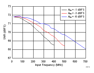
The ADS54J42 has a thermal noise of approximately 71.1 dBFS and an internal aperture jitter of 120 fS. SNR, depending on the amount of external jitter for different input frequencies, is shown in Figure 132.
The ADS54J42 is designed for wideband receiver applications demanding excellent dynamic range over a large input frequency range. A typical schematic for an ac-coupled receiver is shown in Figure 133.
NOTE:
GND = AGND and DGND are connected in the PCB layout.Typical applications involving transformer-coupled circuits are discussed in this section. Transformers (such as ADT1-1WT or WBC1-1) can be used up to 300 MHz to achieve good phase and amplitude balances at the ADC inputs. When designing dc-driving circuits, the ADC input impedance must be considered. Figure 134 and Figure 135 show the impedance (ZIN = RIN || CIN) across the ADC input pins.
By using the simple drive circuit of Figure 136, uniform performance can be obtained over a wide frequency range. The buffers present at the analog inputs of the device help isolate the external drive source from the switching currents of the sampling circuit.
For optimum performance, the analog inputs must be driven differentially. This architecture improves common-mode noise immunity and even-order harmonic rejection. A small resistor (5 Ω to 10 Ω) in series with each input pin is recommended to damp out ringing caused by package parasitics, as shown in Figure 136.
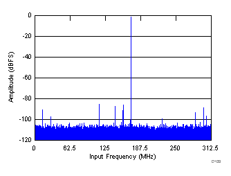
Figure 137 and Figure 138 show the typical performance at 170 MHz and 230 MHz, respectively.
SNR = 71 dBFS, SINAD = 70.9 dBFS, SFDR = 85 dBc, THD = 84 dBc, IL spur = 87 dBc, non HD2, HD3 spur = 93 dBc |
SNR = 70.4 dBFS, SINAD = 69.9 dBFS, IL spur = 89 dBc, SFDR = 80 dBc, THD = 79 dBc, non HD2, HD3 spur = 91 dBc |