-
ADS54J69 Dual-Channel, 16-Bit, 500-MSPS, Analog-to-Digital Converter
- 1 Features
- 2 Applications
- 3 Description
- 4 Revision History
- 5 Device Comparison Table
- 6 Pin Configuration and Functions
- 7 Specifications
-
8 Detailed Description
- 8.1 Overview
- 8.2 Functional Block Diagram
- 8.3 Feature Description
- 8.4 Device Functional Modes
- 8.5
Register Maps
- 8.5.1 Detailed Register Info
- 8.5.2 Example Register Writes
- 8.5.3
Register Descriptions
- 8.5.3.1 General Registers
- 8.5.3.2
Master Page (080h) Registers
- 8.5.3.2.1 Register 20h (address = 20h), Master Page (080h)
- 8.5.3.2.2 Register 21h (address = 21h), Master Page (080h)
- 8.5.3.2.3 Register 23h (address = 23h), Master Page (080h)
- 8.5.3.2.4 Register 24h (address = 24h), Master Page (080h)
- 8.5.3.2.5 Register 26h (address = 26h), Master Page (080h)
- 8.5.3.2.6 Register 39h (address = 39h), Master Page (080h)
- 8.5.3.2.7 Register 3Ah (address = 3Ah), Master Page (080h)
- 8.5.3.2.8 Register 4Fh (address = 4Fh), Master Page (080h)
- 8.5.3.2.9 Register 53h (address = 53h), Master Page (080h)
- 8.5.3.2.10 Register 54h (address = 54h), Master Page (080h)
- 8.5.3.2.11 Register 55h (address = 55h), Master Page (080h)
- 8.5.3.2.12 Register 56h (address = 56h), Master Page (080h)
- 8.5.3.2.13 Register 59h (address = 59h), Master Page (080h)
- 8.5.3.3 ADC Page (0Fh) Registers
- 8.5.3.4
Main Digital Page (6800h) Registers
- 8.5.3.4.1 Register 0h (address = 0h), Main Digital Page (6800h)
- 8.5.3.4.2 Register 41h (address = 41h), Main Digital Page (6800h)
- 8.5.3.4.3 Register 42h (address = 42h), Main Digital Page (6800h)
- 8.5.3.4.4 Register 43h (address = 43h), Main Digital Page (6800h)
- 8.5.3.4.5 Register 44h (address = 44h), Main Digital Page (6800h)
- 8.5.3.4.6 Register 4Bh (address = 4Bh), Main Digital Page (6800h)
- 8.5.3.4.7 Register 4Dh (address = 4Dh), Main Digital Page (6800h)
- 8.5.3.4.8 Register 4Eh (address = 4Eh), Main Digital Page (6800h)
- 8.5.3.4.9 Register 52h (address = 52h), Main Digital Page (6800h)
- 8.5.3.4.10 Register 72h (address = 72h), Main Digital Page (6800h)
- 8.5.3.4.11 Register ABh (address = ABh), Main Digital Page (6800h)
- 8.5.3.4.12 Register ADh (address = ADh), Main Digital Page (6800h)
- 8.5.3.4.13 Register F7h (address = F7h), Main Digital Page (6800h)
- 8.5.3.5
JESD Digital Page (6900h) Registers
- 8.5.3.5.1 Register 0h (address = 0h), JESD Digital Page (6900h)
- 8.5.3.5.2 Register 1h (address = 1h), JESD Digital Page (6900h)
- 8.5.3.5.3 Register 2h (address = 2h), JESD Digital Page (6900h)
- 8.5.3.5.4 Register 3h (address = 3h), JESD Digital Page (6900h)
- 8.5.3.5.5 Register 5h (address = 5h), JESD Digital Page (6900h)
- 8.5.3.5.6 Register 6h (address = 6h), JESD Digital Page (6900h)
- 8.5.3.5.7 Register 7h (address = 7h), JESD Digital Page (6900h)
- 8.5.3.5.8 Register 31h (address = 31h), JESD Digital Page (6900h)
- 8.5.3.5.9 Register 32h (address = 32h), JESD Digital Page (6900h)
- 8.5.3.6 JESD Analog Page (6A00h) Register
- 9 Application and Implementation
- 10Power Supply Recommendations
- 11Layout
- 12Device and Documentation Support
- 13Mechanical, Packaging, and Orderable Information
- IMPORTANT NOTICE
Package Options
Mechanical Data (Package|Pins)
- RMP|72
Thermal pad, mechanical data (Package|Pins)
Orderable Information
ADS54J69 Dual-Channel, 16-Bit, 500-MSPS, Analog-to-Digital Converter
1 Features
- 16-Bit Resolution, Dual-Channel, 500-MSPS ADC
- Idle Channel Noise Floor: –159 dBFS/Hz
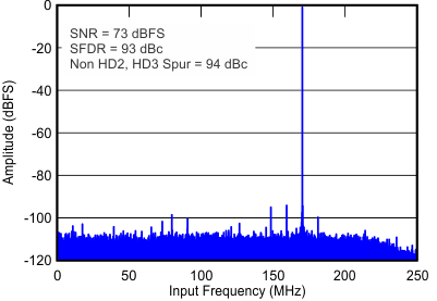
- Spectral Performance (fIN = 170 MHz at –1 dBFS):
- SNR: 73 dBFS
- NSD: –157 dBFS/Hz
- SFDR: 93 dBc
- SFDR: 94 dBc (Except HD2, HD3, and Interleaving Tone)
- Spectral Performance (fIN = 310 MHz at –1 dBFS):
- SNR: 71.7 dBFS
- NSD: –155.7 dBFS/Hz
- SFDR: 81 dBc
- SFDR: 94 dBc (Except HD2, HD3, and Interleaving Tone)
- Channel Isolation: 100 dBc at fIN = 170 MHz
- Input Full-Scale: 1.9 VPP
- Input Bandwidth (3 dB): 1.2 GHz
- On-Chip Dither
- Integrated Decimate-by-2 Filter
- JESD204B Interface with Subclass 1 Support:
- 1 Lane per ADC at 10.0 Gbps
- 2 Lanes per ADC at 5.0 Gbps
- Support for Multi-Chip Synchronization
- Power Dissipation: 1.35 W/ch at 500 MSPS
- 72-Pin VQFNP Package (10 mm × 10 mm)
2 Applications
- Radar and Antenna Arrays
- Broadband Wireless
- Cable CMTS, DOCSIS 3.1 Receivers
- Communications Test Equipment
- Microwave Receivers
- Software Defined Radio (SDR)
- Digitizers
- Medical Imaging and Diagnostics
3 Description
The ADS54J69 is a low-power, wide-bandwidth, 16-bit, 500-MSPS, dual-channel, analog-to-digital converter (ADC). Designed for high signal-to-noise ratio (SNR), the device delivers a noise floor of –159 dBFS/Hz for applications aiming for highest dynamic range over a wide instantaneous bandwidth. The device supports the JESD204B serial interface with data rates up to 10.0 Gbps, supporting one or two lanes per ADC. The buffered analog input provides uniform input impedance across a wide frequency range and minimizes sample-and-hold glitch energy. Each ADC channel is directly connected to a wideband digital down-converter (DDC) block. The ADS54J69 provides excellent spurious-free dynamic range (SFDR) over a large input frequency range with very low power consumption.
The JESD204B interface reduces the number of interface lines, allowing high system integration density. An internal phase-locked loop (PLL) multiplies the ADC sampling clock to derive the bit clock that is used to serialize the 16-bit data from each channel.
Device Information
| PART NUMBER | PACKAGE | BODY SIZE (NOM) |
|---|---|---|
| ADS54J69 | VQFNP (72) | 10.00 mm × 10.00 mm |
- For all available packages, see the orderable addendum at the end of the data sheet.
Spectrum at 170-MHz IF
4 Revision History
Changes from B Revision (February 2016) to C Revision
- Added Device Comparison TableGo
- Added the FOVR latency parameter to the Timing Characteristics tableGo
- Added SYSREF Not Present (Subclass 0, 2) sectionGo
- Changed the number of clock cycles in the Fast OVR sectionGo
- Changed the Register MapGo
- Deleted register 39h, 3Ah, and 56h Go
- Changed the SNR versus Input Frequency and External Clock Jitter figureGo
- Changed Power Supply Recommendations section Go
- Added the Power Sequencing and Initialization sectionGo
- Added Documentation Support and Receiving Notification of Documentation Updates sectionsGo
- Added the Receiving Notification of Documentation Updates sectionGo
Changes from A Revision (January 2016) to B Revision
- Changed Sample Timing, Aperture jitter parameter in Timing Characteristics table Go
- Changed Table 35Go
- Changed Table 42Go
- Changed Table 44Go
- Changed SNR and Clock Jitter section: changed Figure 130 and last sentence of sectionGo
- Changed Application Curves section Go
Changes from * Revision (May 2015) to A Revision
- Released to production Go
6 Pin Configuration and Functions

Pin Functions
| PIN | I/O | DESCRIPTION | |
|---|---|---|---|
| NAME | NO. | ||
| CLOCK, SYSREF | |||
| CLKINM | 28 | I | Negative differential clock input for the ADC |
| CLKINP | 27 | I | Positive differential clock input for the ADC |
| SYSREFM | 34 | I | Negative external SYSREF input |
| SYSREFP | 33 | I | Positive external SYSREF input |
| CONTROL, SERIAL INTERFACE | |||
| PDN | 50 | I/O | Power-down. Can be configured via an SPI register setting. Can be configured to fast overrange output for channel A via the SPI. |
| RESET | 48 | I | Hardware reset; active high. This pin has an internal 20-kΩ pulldown resistor. |
| SCLK | 6 | I | Serial interface clock input |
| SDIN | 5 | I | Serial interface data input |
| SDOUT | 11 | O | Serial interface data output. Can be configured to fast overrange output for channel B via the SPI. |
| SEN | 7 | I | Serial interface enable |
| DATA INTERFACE | |||
| DA0M | 62 | O | JESD204B serial data negative outputs for channel A |
| DA1M | 59 | ||
| DA2M | 56 | ||
| DA3M | 54 | ||
| DA0P | 61 | O | JESD204B serial data positive outputs for channel A |
| DA1P | 58 | ||
| DA2P | 55 | ||
| DA3P | 53 | ||
| DB0M | 65 | O | JESD204B serial data negative outputs for channel B |
| DB1M | 68 | ||
| DB2M | 71 | ||
| DB3M | 1 | ||
| DB0P | 66 | O | JESD204B serial data positive outputs for channel B |
| DB1P | 69 | ||
| DB2P | 72 | ||
| DB3P | 2 | ||
| SYNC | 63 | I | Synchronization input for JESD204B port |
| INPUT, COMMON MODE | |||
| INAM | 41 | I | Differential analog negative input for channel A |
| INAP | 42 | I | Differential analog positive input for channel A |
| INBM | 14 | I | Differential analog negative input for channel B |
| INBP | 13 | I | Differential analog positive input for channel B |
| VCM | 22 | O | Common-mode voltage, 2.1 V. Note that analog inputs are internally biased to this pin through 600 Ω (effective), no external connection from the VCM pin to the INxP or INxM pin is required. |
| POWER SUPPLY | |||
| AGND | 18, 23, 26, 29, 32, 36, 37 | I | Analog ground |
| AVDD | 9, 12, 15, 17, 25, 30, 35, 38, 40, 43, 44, 46 | I | Analog 1.9-V power supply |
| AVDD3V | 10, 16, 24, 31, 39, 45 | I | Analog 3.0-V power supply for the analog buffer |
| DGND | 3, 52, 60, 67 | I | Digital ground |
| DVDD | 8, 47 | I | Digital 1.9-V power supply |
| IOVDD | 4, 51, 57, 64, 70 | I | Digital 1.15-V power supply for the JESD204B transmitter |
| NC, RES | |||
| NC | 19, 20, 21 | — | Unused pins, do not connect |
| RES | 49 | I | Reserved pin. Connect to DGND. |
7 Specifications
7.1 Absolute Maximum Ratings
over operating free-air temperature range (unless otherwise noted)(1)| MIN | MAX | UNIT | ||
|---|---|---|---|---|
| Supply voltage range | AVDD3V | –0.3 | 3.6 | V |
| AVDD | –0.3 | 2.1 | ||
| DVDD | –0.3 | 2.1 | ||
| IOVDD | –0.2 | 1.4 | ||
| Voltage between AGND and DGND | –0.3 | 0.3 | V | |
| Voltage applied to input pins | INAP, INBP, INAM, INBM | –0.3 | 3 | V |
| CLKINP, CLKINM | –0.3 | AVDD + 0.3 | ||
| SYSREFP, SYSREFM | –0.3 | AVDD + 0.3 | ||
| SCLK, SEN, SDIN, RESET, SYNC, PDN | –0.2 | 2.1 | ||
| Storage temperature, Tstg | –65 | 150 | °C | |
7.2 ESD Ratings
| VALUE | UNIT | |||
|---|---|---|---|---|
| V(ESD) | Electrostatic discharge | Human-body model (HBM), per ANSI/ESDA/JEDEC JS-001(1) | ±1000 | V |
| Charged-device model (CDM), per JEDEC specification JESD22-C101(2) | ±500 | |||
7.3 Recommended Operating Conditions
over operating free-air temperature range (unless otherwise noted)(2)(3)| MIN | NOM | MAX | UNIT | |||
|---|---|---|---|---|---|---|
| Supply voltage range | AVDD3V | 2.85 | 3.0 | 3.6 | V | |
| AVDD | 1.8 | 1.9 | 2.0 | |||
| DVDD | 1.7 | 1.9 | 2.0 | |||
| IOVDD | 1.1 | 1.15 | 1.2 | |||
| Analog inputs | Differential input voltage range | 1.9 | VPP | |||
| Input common-mode voltage | 2.0 | V | ||||
| Maximum analog input frequency for 1.9-VPP input amplitude(4)(5) | 400 | MHz | ||||
| Clock inputs | Input clock frequency, device clock frequency | 500 | 1000 | MHz | ||
| Input clock amplitude differential (VCLKP – VCLKM) |
Sine wave, ac-coupled | 0.75 | 1.5 | VPP | ||
| LVPECL, ac-coupled | 0.8 | 1.6 | ||||
| LVDS, ac-coupled | 0.7 | |||||
| Input device clock duty cycle | 45% | 50% | 55% | |||
| Temperature | Operating free-air, TA | –40 | 85 | ºC | ||
| Operating junction, TJ | 105(1) | 125 | ||||
7.4 Thermal Information
| THERMAL METRIC(1) | ADS54J69 | UNIT | |
|---|---|---|---|
| RMP (VQFNP) | |||
| 72 PINS | |||
| RθJA | Junction-to-ambient thermal resistance | 22.3 | °C/W |
| RθJC(top) | Junction-to-case (top) thermal resistance | 5.1 | °C/W |
| RθJB | Junction-to-board thermal resistance | 2.4 | °C/W |
| ψJT | Junction-to-top characterization parameter | 0.1 | °C/W |
| ψJB | Junction-to-board characterization parameter | 2.3 | °C/W |
| RθJC(bot) | Junction-to-case (bottom) thermal resistance | 0.4 | °C/W |
7.5 Electrical Characteristics
typical values are at TA = 25°C, full temperature range is from TMIN = –40°C to TMAX = 85°C, device clock frequency = 1 GSPS, output sampling rate = 500 MSPS, 50% clock duty cycle, AVDD3V = 3.0 V, AVDD = DVDD = 1.9 V, IOVDD = 1.15 V, –1-dBFS differential input, and 0-dB digital gain (unless otherwise noted)| PARAMETER | TEST CONDITIONS | MIN | TYP | MAX | UNIT | ||
|---|---|---|---|---|---|---|---|
| GENERAL | |||||||
| Device clock frequency | 1000 | MSPS | |||||
| Output sample rate | 500 | MSPS | |||||
| Resolution | 16 | Bits | |||||
| POWER SUPPLIES | |||||||
| AVDD3V | 3.0-V analog supply | 2.85 | 3.0 | 3.6 | V | ||
| AVDD | 1.9-V analog supply | 1.8 | 1.9 | 2.0 | V | ||
| DVDD | 1.9-V digital supply | 1.7 | 1.9 | 2.0 | V | ||
| IOVDD | 1.15-V SERDES supply | 1.1 | 1.15 | 1.2 | V | ||
| IAVDD3V | 3.0-V analog supply current | VIN = full-scale on both channels | 293 | 360 | mA | ||
| IAVDD | 1.9-V analog supply current | VIN = full-scale on both channels | 354 | 510 | mA | ||
| IDVDD | 1.9-V digital supply current | Four-lane output mode (default after reset) |
188 | 260 | mA | ||
| IIOVDD | 1.15-V SERDES supply current | 512 | 920 | mA | |||
| Pdis | Total power dissipation | 2.66 | 3.1 | W | |||
| IDVDD | 1.9-V digital supply current | Two-lane output mode | 195 | mA | |||
| IIOVDD | 1.15-V SERDES supply current | 559 | mA | ||||
| Pdis | Total power dissipation | 2.73 | W | ||||
| Global power-down power dissipation | Using the GLOBAL PDN register bit in the master page | 204 | 315 | mW | |||
7.6 AC Characteristics
typical values are at TA = 25°C, full temperature range is from TMIN = –40°C to TMAX = 85°C, device clock frequency = 1 GSPS, output sampling rate = 500 MSPS, 50% clock duty cycle, AVDD3V = 3.0 V, AVDD = DVDD = 1.9 V, IOVDD = 1.15 V, –1-dBFS differential input, and 0-dB digital gain (unless otherwise noted)| PARAMETER | TEST CONDITIONS | MIN | TYP | MAX | UNIT | |
|---|---|---|---|---|---|---|
| SNR | Signal-to-noise ratio | fIN = 10 MHz, AIN = –1 dBFS | 74.2 | dBFS | ||
| fIN = 140 MHz, AIN = –1 dBFS | 73.4 | |||||
| fIN = 170 MHz, AIN = –1 dBFS | 71.3 | 73 | ||||
| fIN = 210 MHz, AIN = –1 dBFS | 72.7 | |||||
| fIN = 310 MHz, AIN = –1 dBFS | 71.7 | |||||
| fIN = 370 MHz, AIN = –1 dBFS | 70.3 | |||||
| fIN = 470 MHz, AIN = –3 dBFS | 70.5 | |||||
| NSD | Noise spectral density | fIN = 10 MHz, AIN = –1 dBFS | 158.2 | dBFS/Hz | ||
| fIN = 140 MHz, AIN = –1 dBFS | 157.4 | |||||
| fIN = 170 MHz, AIN = –1 dBFS | 155.3 | 157.0 | ||||
| fIN = 210 MHz, AIN = –1 dBFS | 156.7 | |||||
| fIN = 310 MHz, AIN = –1 dBFS | 155.7 | |||||
| fIN = 370 MHz, AIN = –1 dBFS | 154.3 | |||||
| fIN = 470 MHz, AIN = –3 dBFS | 154.5 | |||||
| SINAD | Signal-to-noise and distortion ratio | fIN = 10 MHz, AIN = –1 dBFS | 73.8 | dBFS | ||
| fIN = 140 MHz, AIN = –1 dBFS | 73.3 | |||||
| fIN = 170 MHz, AIN = –1 dBFS | 69.8 | 72.9 | ||||
| fIN = 210 MHz, AIN = –1 dBFS | 72.5 | |||||
| fIN = 310 MHz, AIN = –1 dBFS | 71.2 | |||||
| fIN = 370 MHz, AIN = –1 dBFS | 70.2 | |||||
| fIN = 470 MHz, AIN = –3 dBFS | 69.4 | |||||
| SFDR | Spurious free dynamic range (excluding IL spurs) | fIN = 10 MHz, AIN = –1 dBFS | 86 | dBc | ||
| fIN = 140 MHz, AIN = –1 dBFS | 95 | |||||
| fIN = 170 MHz, AIN = –1 dBFS | 79 | 94 | ||||
| fIN = 210 MHz, AIN = –1 dBFS | 89 | |||||
| fIN = 310 MHz, AIN = –1 dBFS | 81 | |||||
| fIN = 370 MHz, AIN = –1 dBFS | 87 | |||||
| fIN = 470 MHz, AIN = –3 dBFS | 73 | |||||
| HD2 | Second-order harmonic distortion | fIN = 10 MHz, AIN = –1 dBFS | 86 | dBc | ||
| fIN = 140 MHz, AIN = –1 dBFS | 104 | |||||
| fIN = 170 MHz, AIN = –1 dBFS | 85 | 102 | ||||
| fIN = 210 MHz, AIN = –1 dBFS | 95 | |||||
| fIN = 310 MHz, AIN = –1 dBFS | 81 | |||||
| fIN = 370 MHz, AIN = –1 dBFS | 87 | |||||
| fIN = 470 MHz, AIN = –3 dBFS | 96 | |||||
| HD3 | Third-order harmonic distortion | fIN = 10 MHz, AIN = –1 dBFS | 89 | dBc | ||
| fIN = 140 MHz, AIN = –1 dBFS | 103 | |||||
| fIN = 170 MHz, AIN = –1 dBFS | 86 | 101 | ||||
| fIN = 210 MHz, AIN = –1 dBFS | 100 | |||||
| fIN = 310 MHz, AIN = –1 dBFS | 98 | |||||
| fIN = 370 MHz, AIN = –1 dBFS | 95 | |||||
| fIN = 470 MHz, AIN = –3 dBFS | 73 | |||||
| Non HD2, HD3 |
Spurious-free dynamic range (excluding HD2, HD3, and IL spur) |
fIN = 10 MHz, AIN = –1 dBFS | 98 | dBc | ||
| fIN = 140 MHz, AIN = –1 dBFS | 95 | |||||
| fIN = 170 MHz, AIN = –1 dBFS | 84 | 94 | ||||
| fIN = 210 MHz, AIN = –1 dBFS | 89 | |||||
| fIN = 310 MHz, AIN = –1 dBFS | 92 | |||||
| fIN = 370 MHz, AIN = –1 dBFS | 97 | |||||
| fIN = 470 MHz, AIN = –3 dBFS | 92 | |||||
| ENOB | Effective number of bits | fIN = 10 MHz, AIN = –1 dBFS | 12 | Bits | ||
| fIN = 140 MHz, AIN = –1 dBFS | 11.9 | |||||
| fIN = 170 MHz, AIN = –1 dBFS | 11.3 | 11.9 | ||||
| fIN = 210 MHz, AIN = –1 dBFS | 11.8 | |||||
| fIN = 310 MHz, AIN = –1 dBFS | 11.5 | |||||
| fIN = 370 MHz, AIN = –1 dBFS | 11.4 | |||||
| fIN = 470 MHz, AIN = –3 dBFS | 11.2 | |||||
| THD | Total harmonic distortion | fIN = 10 MHz, AIN = –1 dBFS | 84 | dBc | ||
| fIN = 140 MHz, AIN = –1 dBFS | 95 | |||||
| fIN = 170 MHz, AIN = –1 dBFS | 79 | 89 | ||||
| fIN = 210 MHz, AIN = –1 dBFS | 85 | |||||
| fIN = 310 MHz, AIN = –1 dBFS | 80 | |||||
| fIN = 370 MHz, AIN = –1 dBFS | 85 | |||||
| fIN = 470 MHz, AIN = –3 dBFS | 72 | |||||
| SFDR_IL | Interleaving spur | fIN = 10 MHz, AIN = –1 dBFS | 90 | dBc | ||
| fIN = 140 MHz, AIN = –1 dBFS | 90 | |||||
| fIN = 170 MHz, AIN = –1 dBFS | 75 | 87 | ||||
| fIN = 210 MHz, AIN = –1 dBFS | 85 | |||||
| fIN = 310 MHz, AIN = –1 dBFS | 85 | |||||
| fIN = 370 MHz, AIN = –1 dBFS | 86 | |||||
| fIN = 470 MHz, AIN = –3 dBFS | 82 | |||||
| IMD3 | Two-tone, third-order intermodulation distortion | fIN1 = 185 MHz, fIN2 = 190 MHz, AIN = –7 dBFS |
86 | dBFS | ||
| fIN1 = 365 MHz, fIN2 = 370 MHz, AIN = –7 dBFS |
79 | |||||
| fIN1 = 465 MHz, fIN2 = 470 MHz, AIN = –10 dBFS |
78 | |||||
7.7 Digital Characteristics
typical values are at TA = 25°C, full temperature range is from TMIN = –40°C to TMAX = 85°C, device clock frequency = 1 GSPS, output sampling rate = 500 MSPS, 50% clock duty cycle, AVDD3V = 3.0 V, AVDD = DVDD = 1.9 V, IOVDD = 1.15 V, –1-dBFS differential input, and 0-dB digital gain (unless otherwise noted)| PARAMETER | TEST CONDITIONS | MIN | TYP | MAX | UNITS | |
|---|---|---|---|---|---|---|
| DIGITAL INPUTS (RESET, SCLK, SEN, SDIN, SYNC, PDN)(1) | ||||||
| VIH | High-level input voltage | All digital inputs support 1.2-V and 1.8-V logic levels | 0.8 | V | ||
| VIL | Low-level input voltage | All digital inputs support 1.2-V and 1.8-V logic levels | 0.4 | V | ||
| IIH | High-level input current | SEN | 0 | µA | ||
| RESET, SCLK, SDIN, PDN, SYNC | 50 | |||||
| IIL | Low-level input current | SEN | 50 | µA | ||
| RESET, SCLK, SDIN, PDN, SYNC | 0 | |||||
| DIGITAL INPUTS (SYSREFP, SYSREFM) | ||||||
| VD | Differential input voltage | 0.35 | 0.45 | 1.4 | V | |
| V(CM_DIG) | Common-mode voltage for SYSREF(4) | 1.3 | V | |||
| DIGITAL OUTPUTS (SDOUT, PDN(3)) | ||||||
| VOH | High-level output voltage | DVDD – 0.1 | DVDD | V | ||
| VOL | Low-level output voltage | 0.1 | V | |||
| DIGITAL OUTPUTS (JESD204B Interface: DxP, DxM)(2) | ||||||
| VOD | Output differential voltage | With default swing setting | 700 | mVPP | ||
| VOC | Output common-mode voltage | 450 | mV | |||
| Transmitter short-circuit current | Transmitter pins shorted to any voltage between –0.25 V and 1.45 V | –100 | 100 | mA | ||
| zos | Single-ended output impedance | 50 | Ω | |||
| Output capacitance | Output capacitance inside the device, from either output to ground |
2 | pF | |||
7.8 Timing Characteristics
typical values are at TA = 25°C, full temperature range is from TMIN = –40°C to TMAX = 85°C, device clock frequency = 1 GSPS, output sampling rate = 500 MSPS, 50% clock duty cycle, AVDD3V = 3.0 V, AVDD = DVDD = 1.9 V, IOVDD = 1.15 V, and –1-dBFS differential input (unless otherwise noted)| MIN | TYP | MAX | UNITS | |||
|---|---|---|---|---|---|---|
| SAMPLE TIMING | ||||||
| Aperture delay | 0.75 | 1.6 | ns | |||
| Aperture delay matching between two channels on the same device | ±70 | ps | ||||
| Aperture delay matching between two devices at the same temperature and supply voltage | ±270 | ps | ||||
| Aperture jitter | Actual jitter of sampling clock buffer | 145 | fS rms | |||
| Effective jitter after decimation filtering | 102 | |||||
| WAKE-UP TIMING | ||||||
| Wake-up time to valid data after coming out of global power-down | 150 | µs | ||||
| LATENCY | ||||||
| Data latency(1): ADC sample to digital output | 134(2) | Input clock cycles | ||||
| OVR latency: ADC sample to OVR bit | 62 | Input clock cycles | ||||
| FOVR latency: ADC sample to FOVR signal on pin | 18 + 4 ns | Input clock cycles | ||||
| tPD | Propagation delay: logic gates and output buffers delay (does not change with fS) | 4 | ns | |||
| SYSREF TIMING | ||||||
| tSU_SYSREF | Setup time for SYSREF, referenced to the input clock falling edge | 300 | 900 | ps | ||
| tH_SYSREF | Hold time for SYSREF, referenced to the input clock falling edge | 100 | ps | |||
| JESD OUTPUT INTERFACE TIMING CHARACTERISTICS | ||||||
| Unit interval | 100 | 400 | ps | |||
| Serial output data rate | 2.5 | 10 | Gbps | |||
| Total jitter for BER of 1E-15 and lane rate = 10 Gbps | 26 | ps | ||||
| Random jitter for BER of 1E-15 and lane rate = 10 Gbps | 0.75 | ps rms | ||||
| Deterministic jitter for BER of 1E-15 and lane rate = 10 Gbps | 12 | ps, pk-pk | ||||
| tR, tF | Data rise time, data fall time: rise and fall times are measured from 20% to 80%, differential output waveform, 2.5 Gbps ≤ bit rate ≤ 10 Gbps |
35 | ps | |||
 Figure 1. SYSREF Timing
 Figure 2. Sample Timing Requirements
7.9 Typical Characteristics
typical values are at TA = 25°C, full temperature range is from TMIN = –40°C to TMAX = 85°C, device clock frequency = 1 GSPS, output sampling rate = 500 MSPS, 50% clock duty cycle, AVDD3V = 3.0 V, AVDD = DVDD = 1.9 V, IOVDD = 1.15 V, and –1-dBFS differential input (unless otherwise noted)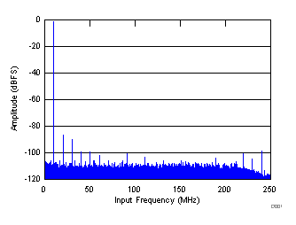
| SNR = 74.2 dBFS; SFDR = 86 dBc; SINAD = 73.8 dBFS; THD = 83 dBc; HD2 = 86 dBc; HD3 = 89 dBc; IL spur = 99 dBc; non HD2, HD3 spur = 98 dBc |
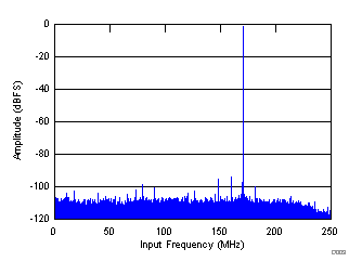
| SNR = 73 dBFS; SFDR = 93 dBc; SINAD = 73.18 dBFS; THD = 89 dBc; HD2 = 93 dBc; HD3 = 103 dBc; IL spur = 99 dBc; non HD2, HD3 spur = 94 dBc |
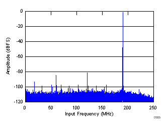
| SNR = 71.6 dBFS; SFDR = 80 dBc; SINAD = 71 dBFS; THD = 79 dBc; HD2 = –80 dBc; HD3 = –96 dBc; IL spur = 85 dBc; non HD2, HD3 spur = 92 dBc |

| SNR = 70.6 dBFS; SFDR = 86 dBc; SINAD = 70.55 dBFS; THD = 85 dBc; tone at –3 dBFS; HD2 = 102 dBc; HD3 = 86 dBc; IL spur = 97 dBc; non HD2, HD3 spur = 96 dBc |

| fIN1 = 185 MHz, fIN2 = 190 MHz, each tone at –36 dBFS, IMD = 101 dBFS |

| fIN1 = 300 MHz, fIN2 = 310 MHz, each tone at –36 dBFS, IMD3 = 102 dBFS |

| fIN1 = 470 MHz, fIN2 = 465 MHz, each tone at –36 dBFS, IMD3 = 104 dBFS |

| fIN1 = 300 MHz, fIN2 = 310 MHz |
Input Amplitude (365 MHz and 370 MHz)

Input Frequency
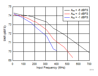

| fIN = 185 MHz |
AVDD Supply and Temperature

| fIN = 300 MHz |
AVDD Supply and Temperature

| fIN = 185 MHz |
DVDD Supply and Temperature

| fIN = 300 MHz |
DVDD Supply and Temperature

| fIN = 185 MHz |
AVDD3V Supply and Temperature
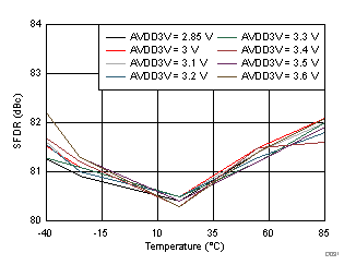
| fIN = 300 MHz |
AVDD3V Supply and Temperature

Gain and Input Frequency

Gain and Input Frequency

| fIN = 185 MHz |

| fIN = 185 MHz |

| fIN = 185 MHz |

| fIN = 185 MHz |

| AIN = –1 dBFS, SFDR = 84 dBc, SINAD = 70 dBFS, fPSRR = 5 MHz, APSRR = 50 mVPP, fIN = 185 MHz, amplitude: fIN – fPSRR = 85 dBc, fIN + fPSRR = 84 dBc |
AVDD Supply

| AIN = –1 dBFS, SFDR = 78 dBc, SINAD = 71 dBFS, fCMRR = 5 MHz, ACMRR = 50 mVPP, fIN = 185 MHz, amplitude: fIN – fCMRR = 79 dBc, fIN + fCMRR = 80 dBc |

Input Frequency

Input Frequency (Output Sample Rate = 300 MSPS)
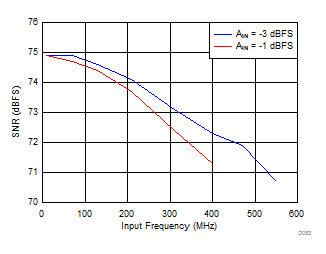
(Output Sample Rate = 350 MSPS)

(Output Sample Rate = 400 MSPS)

| SNR = 73.3 dBFS; SFDR = 94 dBc; SINAD = 73.25 dBFS; THD = 93 dBc; HD2 = 104 dBc; HD3 = 111 dBc; IL spur = 95 dBc; non HD2, HD3 spur = 94 dBc |

| SNR = 72.8 dBFS; SFDR = 89 dBc; SINAD = 72.63 dBFS; THD = 86 dBc; HD2 = 97 dBc; HD3 = 99 dBc; IL spur = 84 dBc; non HD2, HD3 spur = 89 dBc |

| SNR = 70.5 dBFS; SFDR = 86 dBc; SINAD = 70.4 dBFS; THD = 85 dBc; HD2 = –86 dBc; HD3 = –96 dBc; IL spur = 98 dBc; non HD2, HD3 spur = 98 dBc |
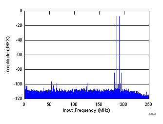
| fIN1 = 185 MHz, fIN2 = 190 MHz, each tone at –7 dBFS, IMD = 86 dBFS |
||

| fIN1 = 300 MHz, fIN2 = 310 MHz, each tone at –7 dBFS, IMD = 79 dBFS |

| fIN1 = 470 MHz, fIN2 = 465 MHz, each tone at –10 dBFS, IMD = 78 dBFS |

| fIN1 = 185 MHz, fIN2 = 190 MHz | ||
Input Amplitude (185 MHz and 190 MHz)

| fIN1 = 465 MHz, fIN2 = 470 MHz |
Input Amplitude (465 MHz and 470 MHz)

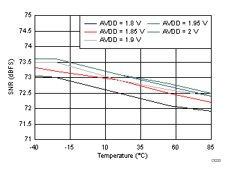
| fIN = 185 MHz |
AVDD Supply and Temperature

| fIN = 300 MHz |
AVDD Supply and Temperature

| fIN = 185 MHz |
DVDD Supply and Temperature
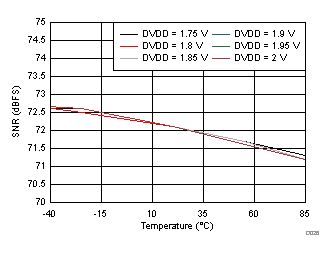
| fIN = 300 MHz |
DVDD Supply and Temperature

| fIN = 185 MHz |
AVDD3V Supply and Temperature

| fIN = 300 MHz |
AVDD3V Supply and Temperature

Gain and Input Frequency

Gain and Input Frequency
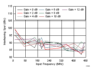

| fIN = 310 MHz |

| fIN = 310 MHz |

| fIN = 310 MHz |

| fIN = 300 MHz |

| fIN = 185 MHz | ||
Noise Signal Frequency

| fIN = 185 MHz | ||
Common-Mode Signal Frequency


Input Frequency (Output Sample Rate = 300 MSPS)

Input Frequency (Output Sample Rate = 350 MSPS)

Input Frequency (Output Sample Rate = 400 MSPS)