SBAS717A June 2015 – June 2015 ADS58J63
PRODUCTION DATA.
- 1 Features
- 2 Applications
- 3 Description
- 4 Revision History
- 5 Pin Configuration and Functions
-
6 Specifications
- 6.1 Absolute Maximum Ratings
- 6.2 ESD Ratings
- 6.3 Recommended Operating Conditions
- 6.4 Thermal Information
- 6.5 Electrical Characteristics
- 6.6 AC Performance
- 6.7 Digital Characteristics
- 6.8 Timing Characteristics
- 6.9 Typical Characteristics: 14-Bit Burst Mode
- 6.10 Typical Characteristics: Mode 2
- 6.11 Typical Characteristics: Mode 0
-
7 Detailed Description
- 7.1 Overview
- 7.2 Functional Block Diagram
- 7.3 Feature Description
- 7.4
Device Functional Modes
- 7.4.1 Digital Features
- 7.4.2 Mode 0 - Decimation by 2 with IQ Outputs for up to 220 MHz of IQ Bandwidth
- 7.4.3 Mode 2 - Decimation by 2 for up to 110 MHz of Real Bandwidth
- 7.4.4 Mode 4/7 - Decimation by 2 with Real Outputs for up to 110 MHz of Bandwidth
- 7.4.5 Mode 5 - Decimation by 2 with IQ Outputs for up to 110 MHz of IQ Bandwidth
- 7.4.6 Mode 6 - Decimation by 4 with IQ Outputs for up to 110 MHz of IQ Bandwidth
- 7.4.7 Mode 8 - Burst Mode
- 7.4.8 Trigger Input
- 7.4.9 Manual Trigger Mode
- 7.4.10 Auto Trigger Mode
- 7.4.11 Over-range Indication
- 7.4.12 Power-Down Mode
- 7.5
Programming
- 7.5.1
Device Configuration
- 7.5.1.1 Details of Serial Interface
- 7.5.1.2 Serial Register Write: Analog Bank
- 7.5.1.3 Serial Register Readout: Analog Bank
- 7.5.1.4 JESD Bank SPI Page Selection
- 7.5.1.5 Serial Register Write: Analog Bank
- 7.5.1.6 Serial Register Readout: Analog Bank
- 7.5.1.7 Digital Bank SPI Page Selection
- 7.5.1.8 Serial Register Write - Digital Bank
- 7.5.1.9 Individual Channel Programming
- 7.5.1.10 Serial Register Readout - Digital Bank
- 7.5.2 JESD204B Interface
- 7.5.1
Device Configuration
- 7.6
Register Maps
- 7.6.1 Detailed Register Info
- 7.6.2 Example Register Writes
- 7.6.3
Register Descriptions
- 7.6.3.1 Register 0h (offset = 0h) [reset = 0h]
- 7.6.3.2 Register 3h/4h (offset = 3h/4h) [reset = 0h]
- 7.6.3.3 Register 5h (offset = 5h) [reset = 0h]
- 7.6.3.4 Register 11h (offset = 11h) [reset = 0h]
- 7.6.3.5
Master Page (80h)
- 7.6.3.5.1 Register 20h (address = 20h) [reset = 0h] , Master Page (080h)
- 7.6.3.5.2 Register 21h (address = 21h) [reset = 0h] , Master Page (080h)
- 7.6.3.5.3 Register 23h (address = 23h), Master Page (080h)
- 7.6.3.5.4 Register 24h (address = 24h) [reset = 0h] , Master Page (080h)
- 7.6.3.5.5 Register 26h (address = 26h), Master Page (080h)
- 7.6.3.5.6 Register 3Ah (address = 3Ah) [reset = 0h] , Master Page (80h)
- 7.6.3.5.7 Register 39h (address = 39h) [reset = 0h] , Master Page (80h)
- 7.6.3.5.8 Register 53h (address = 53h) [reset = 0h] , Master Page (80h)
- 7.6.3.5.9 Register 55h (address = 55h) [reset = 0h] , Master Page (80h)
- 7.6.3.5.10 Register 56h (address = 56h) [reset = 0h] , Master Page (80h)
- 7.6.3.5.11 Register 59h (address = 59h) [reset = 0h] , Master Page (80h)
- 7.6.3.6
ADC Page (0Fh)
- 7.6.3.6.1 Register 5Fh (address = 5Fh) [reset = 0h] , ADC Page (0Fh)
- 7.6.3.6.2 Register 60h (address = 60h) [reset = 0h] , ADC Page (0Fh)
- 7.6.3.6.3 Register 60h (address = 61h) [reset = 0h], ADC Page (0Fh)
- 7.6.3.6.4 Register 6Ch (address = 6Ch) [reset = 0h], ADC Page (0Fh)
- 7.6.3.6.5 Register 6Dh (address = 6Dh) [reset = 0h], ADC Page (0Fh)
- 7.6.3.6.6 Register 74h(address = 74h) [reset = 0h], ADC Page (0Fh)
- 7.6.3.6.7 Register 75h/76h/77h/78h (address = 75h/76h/77h/78h) [reset = 0h], ADC Page (0Fh)
- 7.6.3.7 Interleaving Engine Page (6100h)
- 7.6.3.8 Decimation Filter Page (6141h) Registers
- 7.6.3.9
Main Digital Page (6800h) Registers
- 7.6.3.9.1 Register 0h (address = 0h) [reset = 0h], Main Digital Page (6800h)
- 7.6.3.9.2 Register 42h(address = 42h) [reset = 0h], Main Digital Page (6800h)
- 7.6.3.9.3 Register 4Eh (address = 4Eh) [reset = 0h], Main Digital Page (6800h)
- 7.6.3.9.4 Register ABh (address = ABh) [reset = 0h], Main Digital Page (6800h)
- 7.6.3.9.5 Register ADh (address = ADh) [reset = 0h], Main Digital Page (6800h)
- 7.6.3.9.6 Register F7h (address = F7h) [reset = 0h], Main Digital Page (68h)
- 7.6.3.10
JESD Digital Page (6900h) Registers
- 7.6.3.10.1 Register 0h (address = 0h) [reset = 0h], JESD Digital Page (6900h)
- 7.6.3.10.2 Register 1h (address = 1h) [reset = 0h], JESD Digital Page (6900h)
- 7.6.3.10.3 Register 2h (address = 2h) [reset = 0h], JESD Digital Page (6900h)
- 7.6.3.10.4 Register 3h (address = 3h) [reset = 0h], JESD Digital Page (6900h)
- 7.6.3.10.5 Register 5h (address = 5h) [reset = 0h], JESD Digital Page (6900h)
- 7.6.3.10.6 Register 6h (address = 6h) [reset = 0h], JESD Digital Page (6900h)
- 7.6.3.10.7 Register 17h (address = 17h) [reset = 0h], JESD Digital Page (6900h)
- 7.6.3.10.8 Register 19h/1Ah/1Bh/1Ch (address = 19h/1Ah/1Bh/1Ch) [reset = 0h], JESD Digital Page (6900h)
- 7.6.3.11 JESD Analog Page (6A00h) Register
- 8 Application and Implementation
- 9 Power Supply Recommendations
- 10Layout
- 11Device and Documentation Support
- 12Mechanical, Packaging, and Orderable Information
Package Options
Mechanical Data (Package|Pins)
- RMP|72
Thermal pad, mechanical data (Package|Pins)
Orderable Information
8 Application and Implementation
NOTE
Information in the following applications sections is not part of the TI component specification, and TI does not warrant its accuracy or completeness. TI’s customers are responsible for determining suitability of components for their purposes. Customers should validate and test their design implementation to confirm system functionality.
8.1 Application Information
8.1.1 Start-Up Sequence
The following steps are recommended as the power up sequence with the ADS58J63 in 2x complex decimation mode (DDC Mode 0) with LMFS = 4841 (shown in Table 63).
Table 63. Recommended Power-Up Sequence
| STEP | DESCRIPTION | REGISTER ADDRESS | REGISTER DATA | COMMENT |
|---|---|---|---|---|
| 1 | Supply all supply voltages. There is no required power supply sequence for the 1.15-V supply, 1.9-V supply and 3-V supply, and these may be supplied in any order. | — | — | — |
| 2 | Pulse a hardware reset (low to high to low) on pin 48. | — | — | — |
| Alternatively it can be reset with: Analog reset and Digital reset |
00h 4004h 4003h 4002h 4001h 60F7h |
81h 68h 00h 00h 00h 01h |
||
| 3 | Set input clock divider | 11h 53h |
80h 80h |
Select master page Set clock divider to /2 |
| 4 | Reset interleaving correction engine. Register access default into page 68h | 6000h 6000h |
01h 00h |
Channel AB (and channel CD since device is in broadcast mode) |
| 5 | Default registers for JESD analog page | 4003h 4004h 6016h |
00h 6Ah 02h |
Select JESD analog page m PLL mode 40x for Channel AB and CD |
| 6 | Default registers for JESD digital page | 4003h 4004h 6000h 6006h |
00h 69h 80h 0Fh |
Select JESD digital page m Set CTRL K for channel AB and CD Set K to 16 |
| 7 | Enable single SYNCb input (SYNCAB) | 4005h 7001h |
01h 22h |
Disable broadcast mode Use SYNCAB for channel C/D |
| 8 | Pulse SYNCb (pin 55/56) from low to high to transmit data from k28.5 sync mode | — | — | — |
8.1.2 Hardware Reset
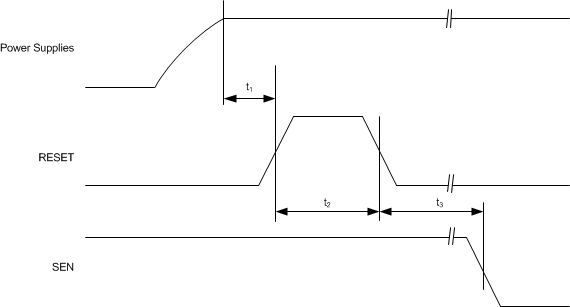
 Figure 138. Hardware Reset Timing Diagram
Table 64. Timing Requirements for Figure 138
| MIN | TYP | MAX | UNIT | |||
|---|---|---|---|---|---|---|
| t1 | Power-on delay | Delay from power up to active high RESET pulse | 1 | ms | ||
| t2 | Reset pulse duration | Active high RESET pulse duration | 10 | ns | ||
| t3 | Register write delay | Delay from RESET disable to SEN active | 100 | ns | ||
8.1.3 SNR and Clock Jitter
The signal to noise ratio of the ADC is limited by three different factors: the quantization noise is typically not noticeable in pipeline converters and is 84 dB for a 14-bit ADC. The thermal noise limits the SNR at low input frequencies while the clock jitter sets the SNR for higher input frequencies.

The SNR limitation resulting from sample clock jitter can be calculated following:

The total clock jitter (TJitter) has two components – the internal aperture jitter (120 fs for ADS58J63) which is set by the noise of the clock input buffer and the external clock jitter. It can be calculated as following:

External clock jitter can be minimized by using high-quality clock sources and jitter cleaners as well as band-pass filters at the clock input while a faster clock slew rate also improves the ADC aperture jitter.
The ADS58J63 has a thermal noise of approximately 72 dBFS and an internal aperture jitter of 120 fs.
8.1.4 ADC Test Pattern
The ADS58J63 provides several different options to output test patterns instead of the actual output data of the ADC in order to simplify bring up of the JESD204B digital interface link. The output data path is shown in Figure 139
 Figure 139. ADC Test Pattern
8.1.4.1 ADC Section
The ADC test pattern replaces the actual output data of the ADC. The following test patterns are available in register 74h. In order to get the test pattern output propoerly, the interleaving correction needs to be disabled (6100h, address 18h) and burst mode enabled (DDC disabled).
Burst mode only supports LMFS = 4421 (DDC Modes have different configurations) and test pattern switches between 9-bit (low resolution) and 14-bit (high resolution) output. See Table 65
Table 65. ADC Test Pattern Settings
| Bit | Name | Default | Description |
|---|---|---|---|
| D7-D4 | TEST PATTERN | 0000 | Test pattern output on channel A and B 0000 Normal Operation using ADC output data 0001 Outputs all 0s 0010 Outputs all 1s 0011 Outputs toggle pattern: Output data are an alternating sequence of 101010101010 and 010101010101 0100 Output digital ramp: output data increments by one LSB every clock cycle from code 0 to 16384 0110 Single pattern: output data is custom pattern 1 (75h and 76h) 0111 Double pattern: output data alternates between custom patter 1 and custom pattern 2 1000 Deskew pattern: output data is 2AAAh 1001 SYNC pattern: output data is 3FFFh |
8.1.4.2 Transport Layer Pattern
The Transport Layer maps the ADC output data into 8bit octets and constructs the JESD204B frames using the LMFS parameters. Tail bits or ‘0’s are added when needed. Alternatively the JESD204B long transport layer test pattern can be substituted as shown in Table 66 .
Table 66. Transport Layer Test-mode
| Bit | Name | Default | Description |
|---|---|---|---|
| D4 | TESTMODE EN | 0 | Generates long transport layer test pattern mode according to clause 5.1.6.3 of JESD204B specification 0 = test mode disabled 1 = test mode enabled |
8.1.4.3 Link Layer Pattern
The Link Layer contains the scrambler and the 8b/10b encoding of any data passed on from the Transport Layer. Additionally it also handles the initial lane alignment sequence which can be manually restarted. The Link Layer test patterns are intended for testing the quality of the link (jitter testing etec). The test patterns do not pass through the 8b/10b encoder and contain the options shown in Table 67.
Table 67. Link Layer Test-mode
| Bit | Name | Default | Description |
|---|---|---|---|
| D7-D5 | LINK LAYER TESTMODE | 000 | Generates pattern according to clause 5.3.3.8.2 of the JESD204B document 000 normal ADC data 001 D21.5 (high frequency jitter pattern) 010 K28.5 (mixed frequency jitter pattern) 011 Repeat initial lane alignment (generates K28.5 character and repeat lane alignment sequences continuously) 100 12 octet RPAT jitter pattern |
Furthermore a 215 PRBS can be enabled by setting up a custom test pattern (AAAA) in the ADC section and running that through the 8b/10b encoder with scrambling enabled.
8.2 Typical Application
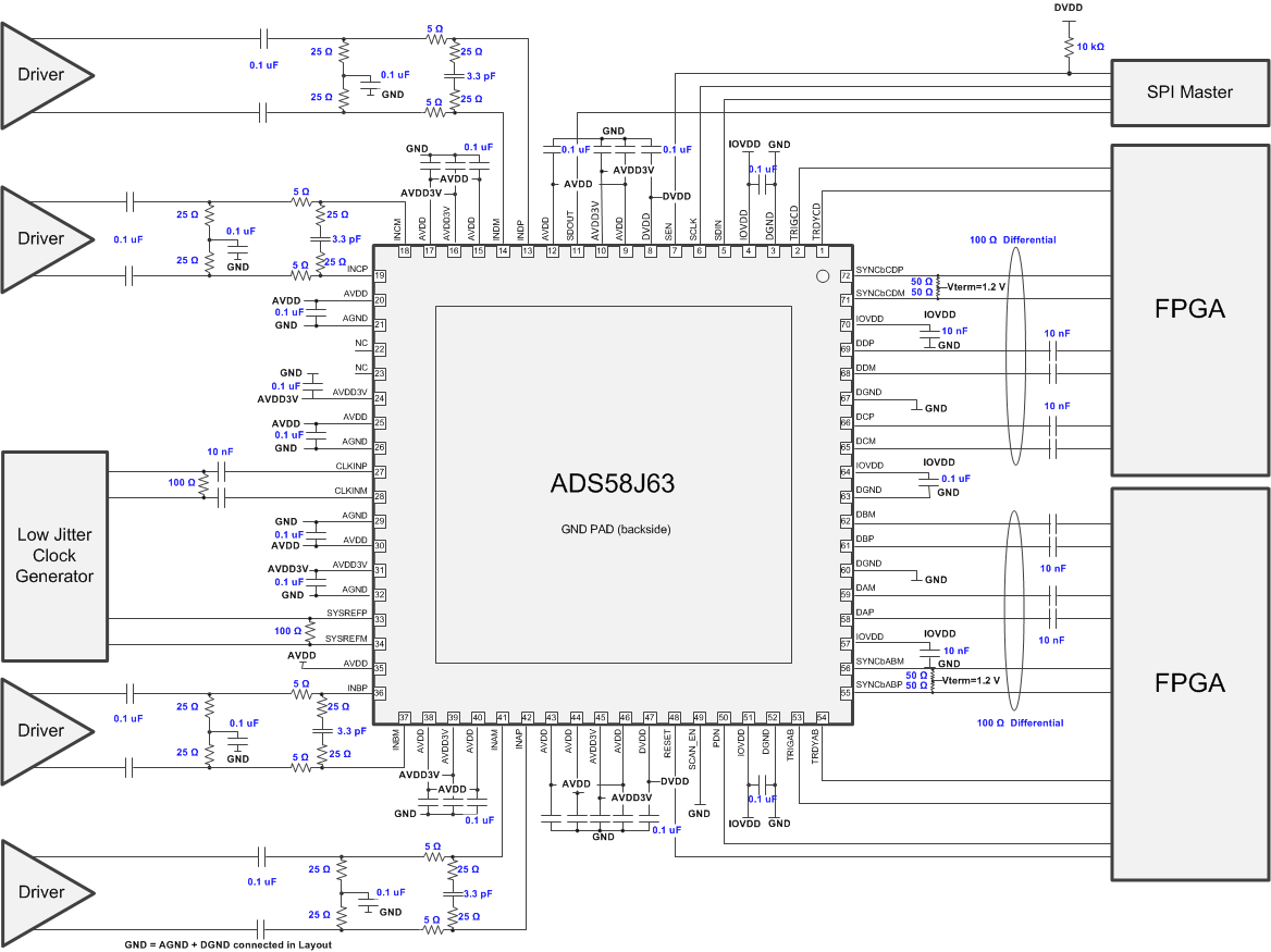
The ADS58J63 is designed for wideband receiver applications demanding excellent dynamic range over a large input frequency range. A typical schematic for an AC coupled dual receiver (dual FPGA with dual SYNC) is shown below.

8.2.1 Design Requirements
By using the simple drive circuit of Figure 140 (when AMP drives ADC) or Figure 51 (when transformers drive ADC), uniform performance can be obtained over a wide frequency range. The buffers present at the analog inputs of the device help isolate the external drive source from the switching currents of the sampling circuit.
8.2.2 Detailed Design Procedure
For optimum performance, the analog inputs must be driven differentially. This architecture improves the common-mode noise immunity and even-order harmonic rejection. A small resistor (5 Ω to 10 Ω) in series with each input pin is recommended to damp out ringing caused by package parasitics, as shown in Figure 140.
8.2.3 Application Curves
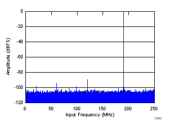
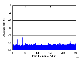
Figure 141 and Figure 142 show the typical performance at 190 MHz and 230 MHz, respectively.

| FIN = 190 MHz , AIN = –1 dBFS SNR = 69.4 dBFS, SFDR = 88 dBc, SFDR = 96 dBc (Non23) |

| FIN = 230 MHz , AIN = –1 dBFS SNR = 69.4 dBFS, SFDR = 85 dBc, SFDR = 96 dBc (Non23) |