SBASAY5 June 2024 ADS8681W
PRODUCTION DATA
- 1
- 1 Features
- 2 Applications
- 3 Description
- 4 Pin Configuration and Functions
- 5 Specifications
-
6 Detailed Description
- 6.1 Overview
- 6.2 Functional Block Diagram
- 6.3 Feature Description
- 6.4 Device Functional Modes
- 6.5 Programming
-
7 Register Maps
- 7.1
Device Configuration and Register Maps
- 7.1.1 DEVICE_ID_REG Register (address = 00h)
- 7.1.2 RST_PWRCTL_REG Register (address = 04h)
- 7.1.3 SDI_CTL_REG Register (address = 08h)
- 7.1.4 SDO_CTL_REG Register (address = 0Ch)
- 7.1.5 DATAOUT_CTL_REG Register (address = 10h)
- 7.1.6 RANGE_SEL_REG Register (address = 14h)
- 7.1.7 ALARM_REG Register (address = 20h)
- 7.1.8 ALARM_H_TH_REG Register (address = 24h)
- 7.1.9 ALARM_L_TH_REG Register (address = 28h)
- 7.1
Device Configuration and Register Maps
- 8 Application and Implementation
- 9 Device and Documentation Support
- 10Revision History
- 11Mechanical, Packaging, and Orderable Information
Package Options
Mechanical Data (Package|Pins)
- RUM|16
Thermal pad, mechanical data (Package|Pins)
- RUM|16
Orderable Information
6.5.1 Data Transfer Frame
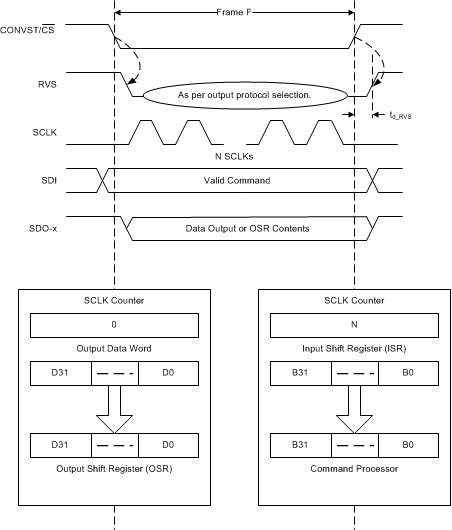
A data transfer frame between the device and the host controller begins at the falling edge of the CONVST/CS pin. This frame ends when the device starts conversions at the subsequent rising edge. The host controller initiates a data transfer frame by bringing the CONVST/CS signal low (Figure 6-25) after the end of the CONV phase. This process is described in the CONV State section.
 Figure 6-25 Data Transfer Frame
For a typical data transfer frame F:
- The host controller pulls
CONVST/CS low to initiate a data transfer frame. On
the falling edge of the CONVST/CS signal:
- RVS goes low, indicating the beginning of the data transfer frame.
- The internal SCLK counter is reset to 0.
- The device takes control of the data bus. As illustrated in Figure 6-25, the contents of the output data word are loaded into the 32-bit output shift register (OSR).
- The internal configuration register is reset to 0000h, corresponding to a NOP command.
- During the frame, the host controller provides clocks on the SCLK pin:
- On each SCLK capture edge, the SCLK counter is incremented. The data bit received on the SDI pin is then shifted into the LSB of the input shift register.
- On each launch edge of the output clock, the MSB of the output shift register data is shifted out on the selected SDO-x pins. In this case the SCLK is the output clock.
- The status of the RVS pin depends on the output protocol selection (see the Protocols for Reading From the Device section).
- The host controller pulls the
CONVST/CS pin high to end the data transfer frame.
On the rising edge of CONVST/CS:
- The SDO-x pins go to tri-state.
- As illustrated in Figure 6-25, the contents of the input shift register are transferred to the command processor for decoding and further action.
- RVS output goes low, indicating the beginning of conversion.
After pulling CONVST/CS high, the host controller monitors for a low-to-high transition on the RVS pin. Alternatively, the host controller waits for the tconv_max time (see the Timing Requirements table) to elapse before initiating a new data transfer frame.
At the end of the data transfer frame F:
- If the SCLK counter is 32, then the device treats the frame F as an optimal data transfer frame for any read or write operation. At the end of an optimal data transfer frame, the command processor treats the 32-bit input shift register contents as a valid command word.
- If the SCLK counter is less than 32, then the
device treats the frame F as a short data transfer frame.
- The data write operation to the device in invalid and the device treats this frame as an NOP command.
- The output data bits transferred during a short frame on the SDO-x pins are still valid data. The host controller uses the short data transfer frame to read only the required number of MSB bits from the 32-bit output shift register.
- If the SCLK counter is greater than 32, then the device treats the frame F as a long data transfer frame. At the end of a long data transfer frame, the command processor treats the 32-bit input shift register contents as a valid command word. There is no restriction on the maximum number of clocks provided within any data transfer frame F. When the host provides a long data transfer frame, the last 32 bits shifted into the device before the CONVST/CS rising edge constitute the desired command.