SBASAY5 June   2024 ADS8681W

PRODUCTION DATA  

  1.   1
  2. Features
  3. Applications
  4. Description
  5. Pin Configuration and Functions
  6. Specifications
    1. 5.1 Absolute Maximum Ratings
    2. 5.2 ESD Ratings
    3. 5.3 Recommended Operating Conditions
    4. 5.4 Thermal Information
    5. 5.5 Electrical Characteristics
    6. 5.6 Timing Requirements
    7. 5.7 Timing Diagrams
    8. 5.8 Typical Characteristics
  7. Detailed Description
    1. 6.1 Overview
    2. 6.2 Functional Block Diagram
    3. 6.3 Feature Description
      1. 6.3.1 Analog Input Structure
      2. 6.3.2 Analog Input Impedance
      3. 6.3.3 Input Protection Circuit
      4. 6.3.4 Programmable Gain Amplifier (PGA)
      5. 6.3.5 Second-Order, Low-Pass Filter (LPF)
      6. 6.3.6 ADC Driver
      7. 6.3.7 Reference
        1. 6.3.7.1 Internal Reference
        2. 6.3.7.2 External Reference
      8. 6.3.8 ADC Transfer Function
      9. 6.3.9 Alarm Features
        1. 6.3.9.1 Input Alarm
        2. 6.3.9.2 AVDD Alarm
    4. 6.4 Device Functional Modes
      1. 6.4.1 Host-to-Device Connection Topologies
        1. 6.4.1.1 Single Device: All multiSPI Options
        2. 6.4.1.2 Single Device: Standard SPI Interface
        3. 6.4.1.3 Multiple Devices: Daisy-Chain Topology
      2. 6.4.2 Device Operational Modes
        1. 6.4.2.1 RESET State
        2. 6.4.2.2 ACQ State
        3. 6.4.2.3 CONV State
    5. 6.5 Programming
      1. 6.5.1 Data Transfer Frame
      2. 6.5.2 Input Command Word and Register Write Operation
      3. 6.5.3 Output Data Word
      4. 6.5.4 Data Transfer Protocols
        1. 6.5.4.1 Protocols for Configuring the Device
        2. 6.5.4.2 Protocols for Reading From the Device
          1. 6.5.4.2.1 Legacy, SPI-Compatible (SYS-xy-S) Protocols With a Single SDO-x
          2. 6.5.4.2.2 Legacy, SPI-Compatible (SYS-xy-S) Protocols With Dual SDO-x
          3. 6.5.4.2.3 Source-Synchronous (SRC) Protocols
            1. 6.5.4.2.3.1 Output Clock Source Options
            2. 6.5.4.2.3.2 Output Bus Width Options
  8. Register Maps
    1. 7.1 Device Configuration and Register Maps
      1. 7.1.1 DEVICE_ID_REG Register (address = 00h)
      2. 7.1.2 RST_PWRCTL_REG Register (address = 04h)
      3. 7.1.3 SDI_CTL_REG Register (address = 08h)
      4. 7.1.4 SDO_CTL_REG Register (address = 0Ch)
      5. 7.1.5 DATAOUT_CTL_REG Register (address = 10h)
      6. 7.1.6 RANGE_SEL_REG Register (address = 14h)
      7. 7.1.7 ALARM_REG Register (address = 20h)
      8. 7.1.8 ALARM_H_TH_REG Register (address = 24h)
      9. 7.1.9 ALARM_L_TH_REG Register (address = 28h)
  9. Application and Implementation
    1. 8.1 Application Information
    2. 8.2 Typical Application
      1. 8.2.1 Design Requirements
      2. 8.2.2 Detailed Design Procedure
        1. 8.2.2.1 Alarm Function
      3. 8.2.3 Application Curve
    3. 8.3 Power Supply Recommendations
      1. 8.3.1 Power Supply Decoupling
      2. 8.3.2 Power Saving
        1. 8.3.2.1 NAP Mode
        2. 8.3.2.2 Power-Down (PD) Mode
    4. 8.4 Layout
      1. 8.4.1 Layout Guidelines
      2. 8.4.2 Layout Example
  10. Device and Documentation Support
    1. 9.1 Documentation Support
      1. 9.1.1 Related Documentation
    2. 9.2 Receiving Notification of Documentation Updates
    3. 9.3 Support Resources
    4. 9.4 Trademarks
    5. 9.5 Electrostatic Discharge Caution
    6. 9.6 Glossary
  11. 10Revision History
  12. 11Mechanical, Packaging, and Orderable Information

Package Options

Mechanical Data (Package|Pins)
Thermal pad, mechanical data (Package|Pins)
Orderable Information

Input Alarm

The device features a high and a low alarm on the analog input. The alarms corresponding to the input signal have independently programmable thresholds and a common hysteresis setting controlled through the ALARM_H_TH_REG and ALARM_L_TH_REG registers.

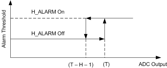
The device sets the input high alarm when the digital output exceeds the high alarm upper limit [high alarm threshold (T)]. The alarm resets when the digital output is less than or equal to the high alarm lower limit [high alarm (T) – H – 1]. Figure 6-17 shows this function.

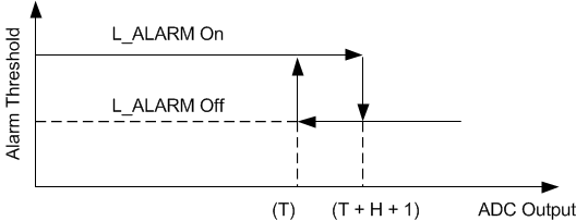
Similarly, the input low alarm is triggered when the digital output falls below the low alarm lower limit [low alarm threshold (T)]. The alarm resets when the digital output is greater than or equal to the low alarm higher limit [low alarm (T) + H + 1]. Figure 6-18 shows this function.
ADS8681W ADS8685W ADS8689W High ALARM Hysteresis
 
Figure 6-17 High ALARM Hysteresis
ADS8681W ADS8685W ADS8689W Low ALARM Hysteresis
 
Figure 6-18 Low ALARM Hysteresis