SBAS707B June 2016 – January 2018 ADS8910B , ADS8912B , ADS8914B
PRODUCTION DATA.
- 1 Features
- 2 Applications
- 3 Description
- 4 Revision History
- 5 Pin Configuration and Functions
- 6 Specifications
-
7 Detailed Description
- 7.1 Overview
- 7.2 Functional Block Diagram
- 7.3 Feature Description
- 7.4 Device Functional Modes
- 7.5
Programming
- 7.5.1 Output Data Word
- 7.5.2 Data Transfer Frame
- 7.5.3 Interleaving Conversion Cycles and Data Transfer Frames
- 7.5.4 Data Transfer Protocols
- 7.5.5 Device Setup
- 7.6
Register Maps
- 7.6.1
Device Configuration and Register Maps
- 7.6.1.1 PD_CNTL Register (address = 04h) [reset = 00h]
- 7.6.1.2 SDI_CNTL Register (address = 008h) [reset = 00h]
- 7.6.1.3 SDO_CNTL Register (address = 0Ch) [reset = 00h]
- 7.6.1.4 DATA_CNTL Register (address = 010h) [reset = 00h]
- 7.6.1.5 PATN_LSB Register (address = 014h) [reset = 00h]
- 7.6.1.6 PATN_MID Register (address = 015h) [reset = 00h]
- 7.6.1.7 PATN_MSB Register (address = 016h) [reset = 00h]
- 7.6.1.8 OFST_CAL Register (address = 020h) [reset = 00h]
- 7.6.1.9 REF_MRG Register (address = 030h) [reset = 00h]
- 7.6.1
Device Configuration and Register Maps
-
8 Application and Implementation
- 8.1 Application Information
- 8.2 Typical Application
- 9 Power-Supply Recommendations
- 10Layout
- 11Device and Documentation Support
- 12Mechanical, Packaging, and Orderable Information
Package Options
Mechanical Data (Package|Pins)
- RGE|24
Thermal pad, mechanical data (Package|Pins)
- RGE|24
Orderable Information
7.5.4.2.1 Legacy, SPI-Compatible (SYS-xy-S) Protocols
As shown in Table 5, the host controller can use any of the four legacy, SPI-compatible protocols (SPI-00-S, SPI-01-S, SPI-10-S, or SPI-11-S) to read data from the device.
Table 5. SPI Protocols for Reading From the Device
| PROTOCOL | SCLK POLARITY (At CS Falling Edge) | SCLK PHASE (Capture Edge) | MSB BIT LAUNCH EDGE | SDI_CNTL | SDO_CNTL | NO. OF SCLK (Optimal Read Frame) | TIMING DIAGRAM |
|---|---|---|---|---|---|---|---|
| SPI-00-S | Low | Rising | CS falling | 00h | 00h | 18 | Figure 54 |
| SPI-01-S | Low | Falling | 1st SCLK rising | 01h | 00h | 18 | Figure 55 |
| SPI-10-S | High | Falling | CS falling | 02h | 00h | 18 | Figure 56 |
| SPI-11-S | High | Rising | 1st SCLK falling | 03h | 00h | 18 | Figure 57 |
At power-up or after coming out of any asynchronous reset, the device supports the SPI-00-S protocol for data-read and data-write operations. To select a different SPI-compatible protocol for both the data transfer operations:
- Program the SDI_MODE[1:0] bits in the SDI_CNTL register. This first write operation must adhere to the SPI-00-S protocol. Any subsequent data transfer frames must adhere to the newly selected protocol.
- Set the SDO_MODE[1:0] bits = 00b in the SDO_CNTL register.
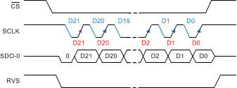
Figure 54 to Figure 57 explain the details of the four protocols using an optimal command frame to read all 22 bits of the output data word. Table 5 shows the number of SCLK required in an optimal read frame for the different output protocol selections.
 Figure 54. SPI-00-S Protocol, 22 SCLKs
 Figure 56. SPI-10-S Protocol, 22 SCLKs
 Figure 55. SPI-01-S Protocol, 22 SCLKs
 Figure 57. SPI-11-S Protocol, 22 SCLKs
For SDI_MODE[1:0] = 00b or 10b, the device supports an Early Data Launch (EDL) option. Set SDO_MODE[1:0] = 01b in the SDO_CNTL register to enable the feature (see Table 6). Setting SDO_MODE[1:0] = 01b has no effect if SDI_MODE[1:0] = 01b or 11b.
Table 6. SPI Protocols with Early Data Launch
| PROTOCOL | SCLK POLARITY (At CS Falling Edge) | SCLK PHASE (Capture Edge) | MSB BIT LAUNCH EDGE | SDI_CNTL | SDO_CNTL | NO. OF SCLK (Optimal Read Frame) | TIMING DIAGRAM |
|---|---|---|---|---|---|---|---|
| SPI-00-S-EDL | Low | Rising | CS falling | 00h | 01h | 18 | Figure 54 |
| SPI-10-S-EDL | High | Falling | CS falling | 02h | 01h | 18 | Figure 56 |
As shown in Figure 58, and Figure 59, the device launches the output data bit on the SDO-0 pin half clock earlier compared to the standard SPI protocol.
 Figure 58. SPI-00-S-EDL Protocol, 22 SCLKs
 Figure 59. SPI-10-S-EDL Protocol, 22 SCLKs
When using these SPI-compatible protocols, the RVS output remains low throughout the data transfer frame; see the Timing Requirements and Switching Characteristics tables for associated timing parameters.
With SDO_CNTL[7:0] = 00h or 01h, if the host controller uses a long data transfer frame, the device exhibits daisy-chain operation (see the Multiple Devices: Daisy-Chain Topology section).
NOTE
Use SPI-compatible protocols to execute the RD_REG, WR_REG, CLR_BITS, and SET_BITS commands specified in Table 2.