SLASF77A December 2022 – September 2023 AFE11612-SEP
PRODUCTION DATA
- 1
- 1 Features
- 2 Applications
- 3 Description
- 4 Revision History
- 5 Pin Configuration and Functions
-
6 Specifications
- 6.1 Absolute Maximum Ratings
- 6.2 ESD Ratings
- 6.3 Recommended Operating Conditions
- 6.4 Thermal Information
- 6.5 Electrical Characteristics
- 6.6 Timing Characteristics
- 6.7 Timing Diagrams
- 6.8 Typical Characteristics: DAC
- 6.9 Typical Characteristics: ADC
- 6.10 Typical Characteristics: Internal Reference
- 6.11 Typical Characteristics: Temperature Sensor
- 6.12 Typical Characteristics: Digital Inputs
-
7 Detailed Description
- 7.1 Overview
- 7.2 Functional Block Diagram
- 7.3
Feature Description
- 7.3.1
Primary ADC Operation
- 7.3.1.1 Analog Inputs
- 7.3.1.2 ADC Trigger Signals (See AFE configuration register 0 )
- 7.3.1.3 Double-Buffered ADC Data Registers
- 7.3.1.4 SCLK Clock Noise Reduction
- 7.3.1.5 Data Available Pin (DAV)
- 7.3.1.6 Convert Pin (CNVT)
- 7.3.1.7 Analog Input Out-of-Range Detection (See The Analog Input Out-of-Range Alarm Section)
- 7.3.1.8 Full-Scale Range of the Analog Input
- 7.3.2 Secondary ADC and Temperature Sensor Operation
- 7.3.3 Reference Operation
- 7.3.4 DAC Operation
- 7.3.5 Alarm Operation
- 7.3.6 General-Purpose Input and Output Pins (GPIO-0 To GPIO-7)
- 7.3.7 Device Reset Options
- 7.3.1
Primary ADC Operation
- 7.4 Device Functional Modes
- 7.5 Programming
- 7.6
Register Maps
- 7.6.1 Temperature Data Registers (Read-Only)
- 7.6.2 Temperature Configuration (TEMP_CONFIG) Register (address = 0Ah) [reset = 003Ch or 3CFFh]
- 7.6.3 Temperature Conversion Rate (TEMP_CONV_RATE) Register (address = 0Bh) [reset = 0007h or 07FFh]
- 7.6.4 η-Factor Correction Registers: D1_N_ADJUST and D2_N_ADJUST (address = 21h and 22h) [reset = 0000h or 00FFh]
- 7.6.5 ADC-n-Data (ADC_n) Registers (addresses = 23h to 32h) [reset = 0000h]
- 7.6.6 DAC-n-Data (DAC_n) Registers (addresses = 33h to 3Eh) [reset = 0000h)
- 7.6.7 DAC-n-CLR-Setting (DAC_n_CLR) Registers (addresses = 3Fh to 4Ah) [reset = 0000h]
- 7.6.8 GPIO Register (address = 4Bh) [reset = 00FFh]
- 7.6.9 AFE Configuration Register 0 (AFE_CONFIG_0) (address = 4Ch) [reset = 2000h]
- 7.6.10 AFE Configuration Register 1 (AFE_CONFIG_1) (Address = 4Dh) [reset = 0070h]
- 7.6.11 Alarm Control Register (ALR_CTRL) (address = 4Eh) [reset = 0000h]
- 7.6.12 STATUS Register (Address = 4Fh) [reset = 0000h]
- 7.6.13 ADC Channel Register 0 (ADC_CH0) (address = 50h) [reset = 0000h]
- 7.6.14 ADC Channel Register 1 (ADC_CH1) (address = 51h) [reset = 0000h]
- 7.6.15 ADC Gain Register (ADC_GAIN) (address = 52h) [reset = FFFFh]
- 7.6.16 AUTO_DAC_CLR_SOURCE Register (address = 53h) [reset = 0004h]
- 7.6.17 AUTO_DAC_CLR_EN Register (address = 54h) [reset = 0000h]
- 7.6.18 SW_DAC_CLR Register (address = 55h) [reset = 0000h]
- 7.6.19 HW_DAC_CLR_EN_0 Register (address = 56h) [reset = 0000h]
- 7.6.20 HW_DAC_CLR_EN_1 Register (address = 57h) [reset = 0000h]
- 7.6.21 DAC Configuration (DAC_CONFIG) Register (address = 58h) [reset = 0000h]
- 7.6.22 DAC Gain (DAC_GAIN) Register (address = 59h) [reset = 0000h]
- 7.6.23 Analog Input Channel Threshold Registers (addresses = 5Ah To 61h)
- 7.6.24
Temperature Threshold Registers
- 7.6.24.1 LT_HIGH_THRESHOLD Register (address = 62h) [reset = 07FFh, +255.875°C]
- 7.6.24.2 LT_LOW_THRESHOLD Register (address = 63h) [reset = 0800h, –256°C]
- 7.6.24.3 D1_HIGH_THRESHOLD Register (address = 64h) [reset = 07FFh, +255.875°C]
- 7.6.24.4 D1_LOW_THRESHOLD Register (address = 65h) [reset = 0800h, –256°C]
- 7.6.24.5 D2_HIGH_THRESHOLD Register (address = 66h) [reset = 07FFh, +255.875°C]
- 7.6.24.6 D2_LOW_THRESHOLD Register (address = 67h) [reset = 0800h, –256°C]
- 7.6.25 Hysteresis Registers
- 7.6.26 Power-Down Register (PWR_DOWN) (address = 6Bh) [reset = 0000h)
- 7.6.27 Device ID Register (DEVICE_ID) (read only address = 6Ch) [reset = 1220h]
- 7.6.28 Software Reset (SW_RST) Register (read or write address = 7Ch) [reset = N/A)
- 8 Application and Implementation
- 9 Device and Documentation Support
- 10Mechanical, Packaging, and Orderable Information
Package Options
Mechanical Data (Package|Pins)
- PAP|64
Thermal pad, mechanical data (Package|Pins)
- PAP|64
Orderable Information
7.3.6 General-Purpose Input and Output Pins (GPIO-0 To GPIO-7)
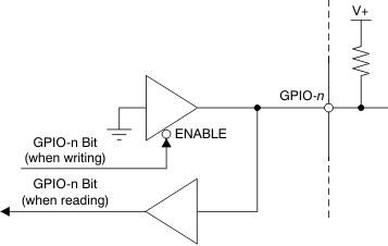
The device has eight GPIO pins. The GPIO-0, GPIO-1, GPIO-2 and GPIO-3 pins are dedicated to general, bidirectional, digital I/O signals. GPIO-4, GPIO-5, GPIO-6, and GPIO-7 are dual-function pins and can be programmed as either bidirectional digital I/O pins or remote temperature sensors D1 and D2. When D1 or D2 is disabled, the pins function as GPIOs. These pins can receive an input or produce an output. When the GPIO-n pin functions as an output, the pin has an open-drain and the status is determined by the corresponding GPIO-n bit of the GPIO register. The output state is high impedance when the GPIO-n bit is set to 1, and is logic low when the GPIO-n bit is cleared (0). A 10-kΩ pullup resistor is required when using the GPIO-n pin as an output; see Figure 7-17. Do not tie the dual-function pins GPIO-4, GPIO-5, GPIO-6, and GPIO-7 to a pullup voltage that exceeds the AVDD supply. The dedicated GPIO-0, GPIO-1, GPIO-2, and GPIO-3 pins are only restricted by the absolute maximum voltage. To use the GPIO-n pin as an input, the corresponding GPIO-n bits in the GPIO register must be set to 1. When the GPIO-n pin functions as an input, the digital value on the pin is acquired by reading the corresponding GPIO-n bit. After a power-on reset or any forced hardware or software reset, all GPIO-n bits are set to 1, and the GPIO-n pin goes to a high-impedance state.
 Figure 7-17 GPIO
Pins