SBASAC2 june 2023 AFE43902-Q1 , AFE53902-Q1
PRODUCTION DATA
- 1
- 1 Features
- 2 Applications
- 3 Description
- 4 Revision History
- 5 Pin Configuration and Functions
-
6 Specifications
- 6.1 Absolute Maximum Ratings
- 6.2 ESD Ratings
- 6.3 Recommended Operating Conditions
- 6.4 Thermal Information
- 6.5 Electrical Characteristics: Voltage Output
- 6.6 Electrical Characteristics: ADC Input
- 6.7 Electrical Characteristics: General
- 6.8 Timing Requirements: I2C Standard Mode
- 6.9 Timing Requirements: I2C Fast Mode
- 6.10 Timing Requirements: I2C Fast Mode Plus
- 6.11 Timing Requirements: SPI Write Operation
- 6.12 Timing Requirements: SPI Read and Daisy Chain Operation (FSDO = 0)
- 6.13 Timing Requirements: SPI Read and Daisy Chain Operation (FSDO = 1)
- 6.14 Timing Requirements: PWM Output
- 6.15 Timing Diagrams
- 6.16 Typical Characteristics: Voltage Output
- 6.17 Typical Characteristics: ADC
- 6.18 Typical Characteristics: General
-
7 Detailed Description
- 7.1 Overview
- 7.2 Functional Block Diagram
- 7.3 Feature Description
- 7.4 Device Functional Modes
- 7.5 Programming
- 7.6
Register Maps
- 7.6.1 NOP Register (address = 00h) [reset = 0000h]
- 7.6.2 DAC-x-VOUT-CMP-CONFIG Register (address = 15h, 03h) [reset = 0400h]
- 7.6.3 COMMON-CONFIG Register (address = 1Fh) [reset = 03F9h]
- 7.6.4 COMMON-TRIGGER Register (address = 20h) [reset = 0000h]
- 7.6.5 COMMON-PWM-TRIG Register (address = 21h) [reset = 0001h]
- 7.6.6 GENERAL-STATUS Register (address = 22h) [reset = 2068h]
- 7.6.7 DEVICE-MODE-CONFIG Register (address = 25h) [reset = 8040h]
- 7.6.8 INTERFACE-CONFIG Register (address = 26h) [reset = 0000h]
- 7.6.9 STATE-MACHINE-CONFIG0 Register (address = 27h) [reset = 0003h]
- 7.6.10 SRAM-CONFIG Register (address = 2Bh) [reset = 0000h]
- 7.6.11 SRAM-DATA Register (address = 2Ch) [reset = 0000h]
- 7.6.12 Xx-TEMPERATURE Register (SRAM address = 20h, 22h, 24h) [reset = 0000h]
- 7.6.13 Yx-TEMPERATURE Register (SRAM address = 21h, 23h, 25h) [reset = 0000h]
- 7.6.14 Xx-OUTPUT Register (SRAM address = 26h, 28h, 2Ah, 2Ch) [reset = 0000h]
- 7.6.15 Yx-OUTPUT Register (SRAM address = 27h, 29h, 2Bh, 2Dh) [reset = 0000h]
- 7.6.16 PWM-FREQUENCY Register (SRAM address = 2Eh) [reset = 0000h]
- 8 Application and Implementation
- 9 Device and Documentation Support
- 10Mechanical, Packaging, and Orderable Information
Package Options
Mechanical Data (Package|Pins)
- RTE|16
Thermal pad, mechanical data (Package|Pins)
- RTE|16
Orderable Information
7.3.4 Power-On Reset (POR)
The AFEx3902-Q1 family of devices includes a power-on reset (POR) function that controls the output voltage at power up. After the VDD supply has been established, a POR event is issued. The POR causes all registers to initialize to default values, and communication with the device is valid only after a POR (boot-up) delay. The default value for all the registers in the AFEx3902-Q1 is loaded from NVM as soon as the POR event is issued.
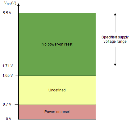
When the device powers up, a POR circuit sets the device to the default mode. The POR circuit requires specific VDD levels, as indicated in Figure 7-2, to make sure that the internal capacitors discharge and reset the device at power up. To make sure that a POR occurs, VDD must be less than 0.7 V for at least 1 ms. When VDD drops to less than 1.65 V, but remains greater than 0.7 V (shown as the undefined region), the device may or may not reset under all specified temperature and power-supply conditions. In this case, initiate a POR. When VDD remains greater than 1.65 V, a POR does not occur.
 Figure 7-2 Threshold Levels for VDD
POR Circuit