-
AFE4404 Ultra-Small, Integrated AFE for Wearable, Optical, Heart-Rate Monitoring and Bio-Sensing
- 1 Features
- 2 Applications
- 3 Description
- 4 Revision History
- 5 Device Comparison Table
- 6 Pin Configuration and Functions
- 7 Specifications
-
8 Detailed Description
- 8.1 Overview
- 8.2 Functional Block Diagram
- 8.3 Feature Description
- 8.4 Device Functional Modes
- 8.5
Register Map
- 8.5.1 Register 0h (address = 0h) [reset = 0h]
- 8.5.2 Register 1h (address = 1h) [reset = 0h]
- 8.5.3 Register 2h (address = 2h) [reset = 0h]
- 8.5.4 Register 3h (address = 3h) [reset = 0h]
- 8.5.5 Register 4h (address = 4h) [reset = 0h]
- 8.5.6 Register 5h (address = 5h) [reset = 0h]
- 8.5.7 Register 6h (address = 6h) [reset = 0h]
- 8.5.8 Register 7h (address = 7h) [reset = 0h]
- 8.5.9 Register 8h (address = 8h) [reset = 0h]
- 8.5.10 Register 9h (address = 9h) [reset = 0h]
- 8.5.11 Register Ah (address = Ah) [reset = 0h]
- 8.5.12 Register Bh (address = Bh) [reset = 0h]
- 8.5.13 Register Ch (address = Ch) [reset = 0h]
- 8.5.14 Register Dh (address = Dh) [reset = 0h]
- 8.5.15 Register Eh (address = Eh) [reset = 0h]
- 8.5.16 Register Fh (address = Fh) [reset = 0h]
- 8.5.17 Register 10h (address = 10h) [reset = 0h]
- 8.5.18 Register 11h (address = 11h) [reset = 0h]
- 8.5.19 Register 12h (address = 12h) [reset = 0h]
- 8.5.20 Register 13h (address = 13h) [reset = 0h]
- 8.5.21 Register 14h (address = 14h) [reset = 0h]
- 8.5.22 Register 15h (address = 15h) [reset = 0h]
- 8.5.23 Register 16h (address = 16h) [reset = 0h]
- 8.5.24 Register 17h (address = 17h) [reset = 0h]
- 8.5.25 Register 18h (address = 18h) [reset = 0h]
- 8.5.26 Register 19h (address = 19h) [reset = 0h]
- 8.5.27 Register 1Ah (address = 1Ah) [reset = 0h]
- 8.5.28 Register 1Bh (address = 1Bh) [reset = 0h]
- 8.5.29 Register 1Ch (address = 1Ch) [reset = 0h]
- 8.5.30 Register 1Dh (address = 1Dh) [reset = 0h]
- 8.5.31 Register 1Eh (address = 1Eh) [reset = 0h]
- 8.5.32 Register 20h (address = 20h) [reset = 0h]
- 8.5.33 Register 21h (address = 21h) [reset = 0h]
- 8.5.34 Register 22h (address = 22h) [reset = 0h]
- 8.5.35 Register 23h (address = 23h) [reset = 0h]
- 8.5.36 Register 29h (address = 29h) [reset = 0h]
- 8.5.37 Register 2Ah (address = 2Ah) [reset = 0h]
- 8.5.38 Register 2Bh (address = 2Bh) [reset = 0h]
- 8.5.39 Register 2Ch (address = 2Ch) [reset = 0h]
- 8.5.40 Register 2Dh (address = 2Dh) [reset = 0h]
- 8.5.41 Register 2Eh (address = 2Eh) [reset = 0h]
- 8.5.42 Register 2Fh (address = 2Fh) [reset = 0h]
- 8.5.43 Register 31h (address = 31h) [reset = 0h]
- 8.5.44 Register 32h (address = 32h) [reset = 0h]
- 8.5.45 Register 33h (address = 33h) [reset = 0h]
- 8.5.46 Register 34h (address = 34h) [reset = 0h]
- 8.5.47 Register 35h (address = 35h) [reset = 0h]
- 8.5.48 Register 36h (address = 36h) [reset = 0h]
- 8.5.49 Register 37h (address = 37h) [reset = 0h]
- 8.5.50 Register 39h (address = 39h) [reset = 0h]
- 8.5.51 Register 3Ah (address = 3Ah) [reset = 0h]
- 8.5.52 Register 3Dh (address = 3Dh) [reset = 0h]
- 8.5.53 Register 3Fh (address = 3Fh) [reset = 0h]
- 8.5.54 Register 40h (address = 40h) [reset = 0h]
- 9 Application and Implementation
- 10Power Supply Recommendations
- 11Layout
- 12Device and Documentation Support
- 13Mechanical, Packaging, and Orderable Information
- IMPORTANT NOTICE
Package Options
Refer to the PDF data sheet for device specific package drawings
Mechanical Data (Package|Pins)
- YZP|15
Thermal pad, mechanical data (Package|Pins)
Orderable Information
AFE4404 Ultra-Small, Integrated AFE for Wearable, Optical, Heart-Rate Monitoring and Bio-Sensing
1 Features
- Transmitter:
- Supports Common Anode LED Configuration
- Dynamic Range: 100 dB
- 6-Bit Programmable LED Current to 50 mA (Extendable to 100 mA)
- Programmable LED On-Time
- Simultaneous Support of 3 LEDs for Optimized SpO2, HRM, or Multi-Wavelength HRM
- Receiver:
- 24-Bit Representation of the Current Input from a Photodiode in Twos Complement Format
- Individual DC Offset Subtraction DAC at TIA Input for Each LED and Ambient Phase
- Digital Ambient Subtraction at ADC Output
- Programmable Transimpedance Gain:
10 kΩ to 2 MΩ - Dynamic Range: 100 dB
- Average Current Less Than 200 μA for PPG Signal Acquisition
- Pulse Frequency: 10 SPS to 1000 SPS
- Flexible Pulse Sequencing and Timing Control
- Flexible Clock Options:
- External Clocking:
4-MHz to 60-MHz Input Clock - Internal Clocking: 4-MHz Oscillator
- External Clocking:
- I2C Interface
- Operating Temperature Range: –20°C to 70°C
- 2.6-mm × 1.6-mm DSBGA Package, 0.5-mm Pitch
- Supplies: Rx: 2 V to 3.6 V, Tx: 3 V to 5.25 V,
IO: 1.8 V to 3.6 V
2 Applications
- Optical Heart-Rate Monitoring (HRM)
- Heart-Rate Variability (HRV)
- Pulse Oximetry (SpO2 Measurement)
- VO2 Max
- Calorie Expenditure
3 Description
The AFE4404 is an analog front-end (AFE) for optical bio-sensing applications, such as heart-rate monitoring (HRM) and saturation of peripheral capillary oxygen (SpO2). The device supports three switching light-emitting diodes (LEDs) and a single photodiode. The current from the photodiode is converted into voltage by the transimpedance amplifier (TIA) and digitized using an analog-to-digital converter (ADC). The ADC code can be read out using an I2C interface. The AFE also has a fully-integrated LED driver with a 6-bit current control. The device has a high dynamic range transmit and receive circuitry that helps with the sensing of very small signal levels.
- For all available packages, see the orderable addendum at the end of the datasheet.
- Refers to dimensions D × E in Figure 99.
Simplified Block Diagram

4 Revision History
Changes from C Revision (May 2016) to D Revision
- Changed last sub-bullet of Receiver Features bullet Go
- Changed test conditions of dynamic power-down mode rows in Current Consumption subsection of Electrical Characteristics tableGo
Changes from B Revision (October 2015) to C Revision
- Changed specifications of t1 and t4 rows in Table 7 to improve rejection of ambient lightGo
- Changed Description column in Table 10 Go
- Changed Table 11Go
- Changed Table 12Go
- Added Reducing Sensitivity to Ambient Light Modulation sectionGo
Changes from A Revision (August 2015) to B Revision
- Changed TX_SUP pin number to E3 in Pin Functions table Go
- Added Figure 9Go
- Added Decimation Mode section Go
- Added rows 3Dh, 3Fh, and 40h to Table 16Go
- Added Register 3Dh description to Register Map sectionGo
- Added Register 3Fh and Register 40h descriptions to Register Map sectionGo
- Added System-Level ESD Considerations section Go
- Added input-referred current paragraph associated to Figure 9 in Application Curves sectionGo
Changes from * Revision (June 2015) to A Revision
5 Device Comparison Table
| PRODUCT | PACKAGE-LEAD | LED DRIVE CONFIGURATION | LED DRIVE CURRENT (mA, Max) |
OPERATING TEMPERATURE RANGE | OPTIMIZED APPLICATION |
|---|---|---|---|---|---|
| AFE4400 | VQFN-40 | H-bridge, common anode |
50 | 0°C to 70°C | Finger-clip pulse oximeters |
| AFE4490 | VQFN-40 | H-bridge, common anode |
200 | –40°C to 85°C | Clinical-grade pulse oximeters |
| AFE4403 | DSBGA-36 | H-bridge, common anode |
100 | –20°C to 70°C | Clinical pulse oximeter patches, wearables |
| AFE4404 | DSBGA-15 | Common anode | 50(1) | –20°C to 70°C | Wearable optical bio-sensing |
6 Pin Configuration and Functions
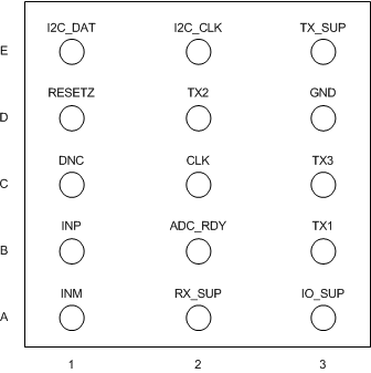
Pin Functions
| PIN | I/O | DESCRIPTION | |
|---|---|---|---|
| NAME | NO. | ||
| ADC_RDY | B2 | Digital | ADC ready interrupt signal (output) |
| CLK | C2 | Digital | Clock input or output, selectable based on register. Default is input (external clock mode). Can be set via a register to output the clock when the oscillator is enabled.(3)(2) |
| DNC | C1 | Do not connect (leave floating) | |
| GND | D3 | Ground | Common ground for transmitter and receiver |
| I2C_CLK | E2 | Digital | I2C clock input, external pullup resistor to IO_SUP (for example, 10 kΩ) |
| I2C_DAT | E1 | Digital | I2C data, external pullup resistor to IO_SUP (for example, 10 kΩ) |
| INM | A1 | Analog | Connect only to anode of photodiode(1) |
| INP | B1 | Analog | Connect only to cathode of photodiode(1) |
| IO_SUP | A3 | Supply | Separate supply for digital I/O. Must be less than or equal to RX_SUP. Can be tied to RX_SUP. |
| RESETZ | D1 | Digital | RESETZ or PWDN: function based on (active low) duration of RESETZ pulse(4). A 25-µs to 50-µs duration = RESETZ active. A > 200-µs duration = PWDN active. |
| RX_SUP | A2 | Supply | Receiver supply; 1-µF decapacitor to GND |
| TX1 | B3 | Analog | Transmit output, LED1 |
| TX2 | D2 | Analog | Transmit output, LED2 |
| TX3 | C3 | Analog | Transmit output, LED3 |
| TX_SUP | E3 | Supply | Transmitter supply; 1-µF decapacitor to GND |
7 Specifications
7.1 Absolute Maximum Ratings
over operating free-air temperature range (unless otherwise noted)(1)| MIN | MAX | UNIT | ||
|---|---|---|---|---|
| Supply voltage range | RX_SUP to GND | –0.3 | 4 | V |
| IO_SUP to GND | –0.3 | 4 | ||
| RX_SUP-IO_SUP | –0.3 | |||
| TX_SUP to GND | –0.3 | 6 | ||
| Voltage applied to analog inputs | Max [–0.3, (GND – 0.3)] | Min [4, (RX_SUP + 0.3)] | V | |
| Voltage applied to digital inputs | Max [–0.3, (GND – 0.3)] | Min [4, (IO_SUP + 0.3)] | V | |
| Maximum duty cycle (cumulative): sum of all LED phase durations as a function of the total period |
50-mA LED current mode (ILED_2X = 0) |
10% | ||
| 100-mA LED current mode (ILED_2X = 1) |
3% | |||
| Storage temperature, Tstg | –60 | 150 | °C | |
7.2 ESD Ratings
| VALUE | UNIT | |||
|---|---|---|---|---|
| V(ESD) | Electrostatic discharge | Human body model (HBM), per ANSI/ESDA/JEDEC JS-001(1) | ±1000 | V |
| Charged device model (CDM), per JEDEC specification JESD22-C101(2) | ±250 | |||
7.3 Recommended Operating Conditions
over operating free-air temperature range (unless otherwise noted)| MIN | MAX | UNIT | |||
|---|---|---|---|---|---|
| RX_SUP | Receiver supply | 2 | 3.6 | V | |
| IO_SUP | Input/output supply | 1.7 | Min (3.6, RX_SUP) | V | |
| TX_SUP | Transmitter supply | 50-mA LED current mode (ILED_2X = 0) |
3.0 or (0.5 + VLED)(1), whichever is greater |
5.25 | V |
| 100-mA LED current mode (ILED_2X = 1) |
3.0 or (1.0 + VLED)(1), whichever is greater |
5.25 | |||
| Digital inputs | 0 | IO_SUP | V | ||
| Analog inputs | 0 | RX_SUP | V | ||
| Operating temperature range | –20 | 70 | °C | ||
7.4 Thermal Information
| THERMAL METRIC(1) | AFE4404 | UNIT | |
|---|---|---|---|
| YZP (DSBGA) | |||
| 15 BALLS | |||
| RθJA | Junction-to-ambient thermal resistance | 67.5 | °C/W |
| RθJC(top) | Junction-to-case (top) thermal resistance | 0.5 | °C/W |
| RθJB | Junction-to-board thermal resistance | 12.9 | °C/W |
| ψJT | Junction-to-top characterization parameter | 0.2 | °C/W |
| ψJB | Junction-to-board characterization parameter | 12.9 | °C/W |
7.5 Electrical Characteristics
Minimum and maximum specifications are at TA = –20°C to 70°C, typical specifications are at 25°C. TX_SUP = 4 V, RX_SUP = IO_SUP = 3 V, 100-Hz PRF, 8-MHz external clock (with CLKDIV_EXTMODE set to divide-by-2), detector CIN = 50 pF, and CLKDIV_PRF set to 1, unless otherwise noted.| PARAMETER | TEST CONDITIONS | MIN | TYP | MAX | UNIT | |
|---|---|---|---|---|---|---|
| PULSE REPETITION FREQUENCY | ||||||
| PRF(1) | Pulse repetition frequency | 10(7) | 1000 | SPS | ||
| RECEIVER | ||||||
| Offset cancellation DAC current range | –7 to 7 | µA | ||||
| Offset cancellation DAC current step | 0.47 | µA | ||||
| TIA gain setting | 10k to 2M | Ω | ||||
| Cf setting | 2.5 to 25 | pF | ||||
| Switched RC filter bandwidth | 2.5(2) | kHz | ||||
| ADC averages | 1 | 16 | ||||
| Detector capacitance | Differential capacitance between INP, INN | 10 | 200 | pF | ||
| TRANSMITTER | ||||||
| LED current range | ILED_2X = 0 | 0 to 50 | mA | |||
| ILED_2X = 1 | 0 to 100 | |||||
| LED current resolution | 6 | Bits | ||||
| CLOCKING (Internal Oscillator) | ||||||
| Frequency | 4 | MHz | ||||
| Accuracy | Room temperature | ±1% | ||||
| Frequency drift with temperature | Full temperature range | ±0.5% | ||||
| Jitter (RMS) | 100 | ps | ||||
| Output clock high level | IO_SUP | V | ||||
| Output clock low level | 0 | V | ||||
| Output clock rise and fall times | 10% to 90%, 15-pF load capacitance on CLK pin |
< 30 | ns | |||
| CLOCKING (External Clock) | ||||||
| Frequency range(3) | 4 | 60 | MHz | |||
| Input clock high level | IO_SUP | V | ||||
| Input clock low level | 0 | V | ||||
| Input capacitance of CLK pin | Capacitance to ground | < 4 | pF | |||
| I2C INTERFACE | ||||||
| Maximum clock speed | 400 | kHz | ||||
| I2C slave address | 58 | Hex | ||||
| PERFORMANCE | ||||||
| Receiver SNR | SNR over a 20-Hz bandwidth for a 500-kΩ gain setting, 50% FS output, 2% LED and sampling pulse duration, ADC averages set to 16 |
100 | dBFS(6) | |||
| Transmitter SNR | SNR over a 20-Hz bandwidth for a 50-mA LED current setting | 100 | dBFS(6) | |||
| CURRENT CONSUMPTION | ||||||
| RX_SUP current | Normal operation, in dynamic power-down mode(8) | 300 | µA | |||
| Always ON receiver, external clock mode | 620 | |||||
| Always ON receiver, internal oscillator mode | 670 | |||||
| Hardware power-down (PWDN) mode(9) | 3 | |||||
| Software power-down (PDNAFE) mode(9) | 35 | |||||
| IO_SUP current | Normal operation, in dynamic power-down mode(8) | 20 | µA | |||
| Always ON receiver, external clock mode | 20 | |||||
| Always ON receiver, internal oscillator mode | 5 | |||||
| Hardware power-down (PWDN) mode(9) | 3 | |||||
| Software power-down (PDNAFE) mode(9) | 5 | |||||
| TX_SUP current | Normal operation, in dynamic power-down mode(8)(10) | 5 | µA | |||
| Always ON receiver, external clock mode(10) | 25 | |||||
| Always ON receiver, internal oscillator mode(10) | 25 | |||||
| Hardware power-down (PWDN) mode(9)(10) | 2 | |||||
| Software power-down (PDNAFE) mode(9)(10) | 2 | |||||
| TRANSIENT RECOVERY | ||||||
| tACTIVE | Recovery from PWDN mode | Time for signal chain to be functional(4) | 10 | ms | ||
| tCHANNEL | Recovery from any event causing a change in signal characteristics | PRF = 100 Hz, sampling duty cycle (each phase) of 2%(5) |
200 | ms | ||
| DIGITAL INPUTS | ||||||
| VIH | High-level input voltage | 0.9 × IO_SUP | IO_SUP | V | ||
| VIL | Low-level input voltage | 0 | 0.1 × IO_SUP | V | ||
| DIGITAL OUTPUTS | ||||||
| VOH | High-level output voltage | IO_SUP | V | |||
| VOL | Low-level output voltage | 0 | V | |||
7.6 Timing Requirements
| MIN | TYP | MAX | UNIT | ||
|---|---|---|---|---|---|
| tI2C_RISE | I2C data rise time with a 10-kΩ pullup resistor with a 20-pF load from I2C data to GND | 1200 | ns | ||
| tI2C_FALL | I2C data fall time (when the data line is pulled down by the AFE) with a 20-pF load from I2C data to GND | 28 | ns | ||
| tADC_RDY_RISE | ADC_RDY rise time (10% to 90%) with a 15-pF capacitive load to ground | 21 | ns | ||
| tADC_RDY_FALL | ADC_RDY fall time (90% to 10%) with a 15-pF capacitive load to ground | 21 | ns | ||
7.7 Typical Characteristics
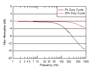
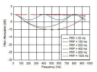
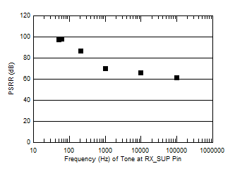
At 25°C, TX_SUP = 4 V, RX_SUP = IO_SUP = 3.3 V, 100-Hz PRF, 25% duty cycle, Rf = 500 kΩ, Cf is adjusted to keep the TIA time constant at 1/10th of the sampling duration, 8-MHz external clock (with CLKDIV_EXTMODE set to divide-by-2), CLKDIV_PRF = 1, detector CIN = 50 pF, ADC averaging = max allowed, SNR (dBFS) = noise referred to full-scale range of 2 V, noise integrated from 1 Hz to Nyquist (= PRF / 2), and values assigned to CLKDIV_EXTMODE and CLK_DIV_PRF parameters correspond to division ratios controlled by these modes, unless otherwise specified.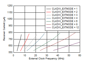
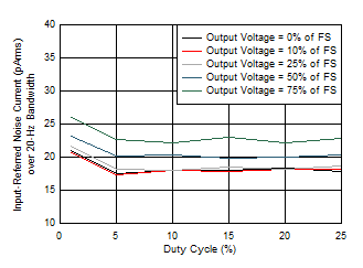
| Duty cycle (x-axis) refers to the sampling duration expressed as a percentage of the pulse repetition period. |
(As a Percentage of Full-Scale)
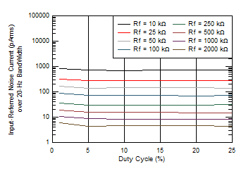
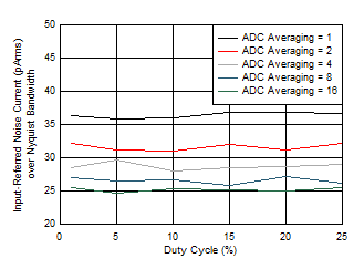
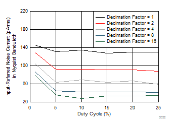 Figure 9. Input-Referred Noise Current in Nyquist Bandwidth vs Duty Cycle (Different Decimation Factor)
| PRF = 2000 Hz |
at the AFE Output
5% Duty Cycle
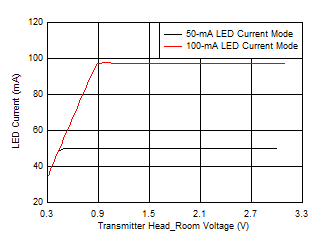
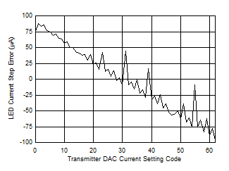
100-mA Mode
| Duty cycle = 1% |
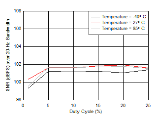
Duty Cycle Across Different Temperatures
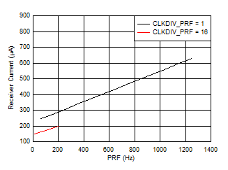
| Active window = 500 µs, LED pulse = 100 µs, all four DYNAMIC bits set to 1 |
Dynamic Power-Down Mode

| Duty cycle (x-axis) refers to the sampling duration expressed as a percentage of the pulse repetition period. |
(As a Percentage of Full-Scale)
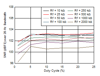
(Different TIA Gain Settings)
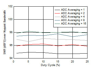
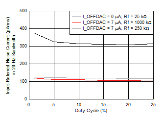
(Different Offset Cancellation DAC Currents)
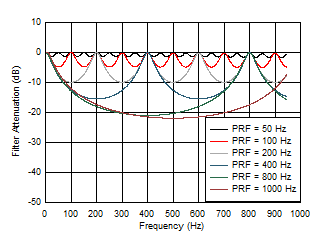
1% Duty Cycle
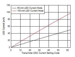
50-mA Mode
| Duty cycle = 1% |
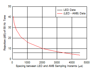
| PRF = 200 Hz, NUMAV = 0 |
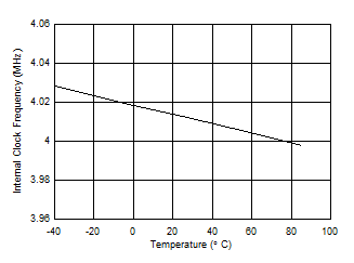
Temperature on a Typical Unit