SBAS689D June 2015 – December 2016 AFE4404
PRODUCTION DATA.
- 1 Features
- 2 Applications
- 3 Description
- 4 Revision History
- 5 Device Comparison Table
- 6 Pin Configuration and Functions
- 7 Specifications
-
8 Detailed Description
- 8.1 Overview
- 8.2 Functional Block Diagram
- 8.3 Feature Description
- 8.4 Device Functional Modes
- 8.5
Register Map
- 8.5.1 Register 0h (address = 0h) [reset = 0h]
- 8.5.2 Register 1h (address = 1h) [reset = 0h]
- 8.5.3 Register 2h (address = 2h) [reset = 0h]
- 8.5.4 Register 3h (address = 3h) [reset = 0h]
- 8.5.5 Register 4h (address = 4h) [reset = 0h]
- 8.5.6 Register 5h (address = 5h) [reset = 0h]
- 8.5.7 Register 6h (address = 6h) [reset = 0h]
- 8.5.8 Register 7h (address = 7h) [reset = 0h]
- 8.5.9 Register 8h (address = 8h) [reset = 0h]
- 8.5.10 Register 9h (address = 9h) [reset = 0h]
- 8.5.11 Register Ah (address = Ah) [reset = 0h]
- 8.5.12 Register Bh (address = Bh) [reset = 0h]
- 8.5.13 Register Ch (address = Ch) [reset = 0h]
- 8.5.14 Register Dh (address = Dh) [reset = 0h]
- 8.5.15 Register Eh (address = Eh) [reset = 0h]
- 8.5.16 Register Fh (address = Fh) [reset = 0h]
- 8.5.17 Register 10h (address = 10h) [reset = 0h]
- 8.5.18 Register 11h (address = 11h) [reset = 0h]
- 8.5.19 Register 12h (address = 12h) [reset = 0h]
- 8.5.20 Register 13h (address = 13h) [reset = 0h]
- 8.5.21 Register 14h (address = 14h) [reset = 0h]
- 8.5.22 Register 15h (address = 15h) [reset = 0h]
- 8.5.23 Register 16h (address = 16h) [reset = 0h]
- 8.5.24 Register 17h (address = 17h) [reset = 0h]
- 8.5.25 Register 18h (address = 18h) [reset = 0h]
- 8.5.26 Register 19h (address = 19h) [reset = 0h]
- 8.5.27 Register 1Ah (address = 1Ah) [reset = 0h]
- 8.5.28 Register 1Bh (address = 1Bh) [reset = 0h]
- 8.5.29 Register 1Ch (address = 1Ch) [reset = 0h]
- 8.5.30 Register 1Dh (address = 1Dh) [reset = 0h]
- 8.5.31 Register 1Eh (address = 1Eh) [reset = 0h]
- 8.5.32 Register 20h (address = 20h) [reset = 0h]
- 8.5.33 Register 21h (address = 21h) [reset = 0h]
- 8.5.34 Register 22h (address = 22h) [reset = 0h]
- 8.5.35 Register 23h (address = 23h) [reset = 0h]
- 8.5.36 Register 29h (address = 29h) [reset = 0h]
- 8.5.37 Register 2Ah (address = 2Ah) [reset = 0h]
- 8.5.38 Register 2Bh (address = 2Bh) [reset = 0h]
- 8.5.39 Register 2Ch (address = 2Ch) [reset = 0h]
- 8.5.40 Register 2Dh (address = 2Dh) [reset = 0h]
- 8.5.41 Register 2Eh (address = 2Eh) [reset = 0h]
- 8.5.42 Register 2Fh (address = 2Fh) [reset = 0h]
- 8.5.43 Register 31h (address = 31h) [reset = 0h]
- 8.5.44 Register 32h (address = 32h) [reset = 0h]
- 8.5.45 Register 33h (address = 33h) [reset = 0h]
- 8.5.46 Register 34h (address = 34h) [reset = 0h]
- 8.5.47 Register 35h (address = 35h) [reset = 0h]
- 8.5.48 Register 36h (address = 36h) [reset = 0h]
- 8.5.49 Register 37h (address = 37h) [reset = 0h]
- 8.5.50 Register 39h (address = 39h) [reset = 0h]
- 8.5.51 Register 3Ah (address = 3Ah) [reset = 0h]
- 8.5.52 Register 3Dh (address = 3Dh) [reset = 0h]
- 8.5.53 Register 3Fh (address = 3Fh) [reset = 0h]
- 8.5.54 Register 40h (address = 40h) [reset = 0h]
- 9 Application and Implementation
- 10Power Supply Recommendations
- 11Layout
- 12Device and Documentation Support
- 13Mechanical, Packaging, and Orderable Information
Package Options
Refer to the PDF data sheet for device specific package drawings
Mechanical Data (Package|Pins)
- YZP|15
Thermal pad, mechanical data (Package|Pins)
Orderable Information
10 Power Supply Recommendations
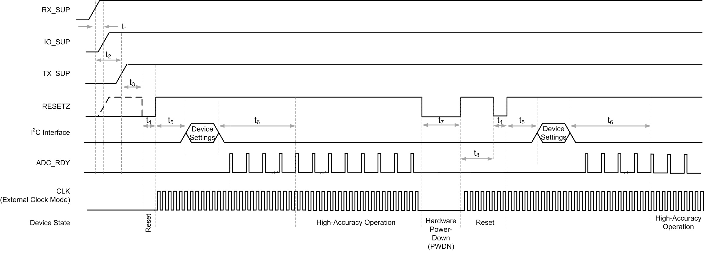
The guidelines for power-supply sequencing and device initialization are shown in Figure 96, Figure 97, and Table 79.
 Figure 96. Power-Supply Sequencing, Device Initialization, and Hardware Power-Down Timing
 Figure 97. Power-Supply Sequencing, Device Initialization, and Software Power-Down Timing
Table 79. Timing Parameters for Power Supply Sequencing, Device Initialization, and Power-Down Timing
| VALUE | ||
|---|---|---|
| t1 | Time between RX_SUP and IO_SUP ramping up | Ramp up RX_SUP before or at the same time as IO_SUP. Keep t1 as small as possible (for example,10 ms). |
| t2 | Time between RX_SUP and TX_SUP ramping up | Keep t2 as small as possible (for example,10 ms). |
| t3 | Time between all supplies stabilizing and start of the RESETZ low-going pulse | > 10 ms |
| t4 | RESETZ pulse duration for the device to get reset | Between 25 µs and 50 µs |
| t5 | Time between resetting the device and issuing of I2C commands | > 1 ms |
| t6 | Time between I2C commands and the ADC_RDY pulse that corresponds to valid data | tCHANNEL(1) |
| t7 | RESETZ pulse duration for the device to enter PWDN (power-down) mode | > 200 µs |
| t8 | Time from exiting power-down mode and subsequently resetting the device | > 10 ms |
(1) The tCHANNEL parameter is specified in the Electrical Characteristics table.