SLASEU7 March   2023 AFE781H1 , AFE881H1

PRODUCTION DATA  

  1. Features
  2. Applications
  3. Description
  4. Revision History
  5. Pin Configuration and Functions
  6. Specifications
    1. 6.1  Absolute Maximum Ratings
    2. 6.2  ESD Ratings
    3. 6.3  Recommended Operating Conditions
    4. 6.4  Thermal Information
    5. 6.5  Electrical Characteristics
    6. 6.6  Timing Requirements
    7. 6.7  Timing Diagrams
    8. 6.8  Typical Characteristics: VOUT DAC
    9. 6.9  Typical Characteristics: ADC
    10. 6.10 Typical Characteristics: Reference
    11. 6.11 Typical Characteristics: HART Modem
    12. 6.12 Typical Characteristics: Power Supply
  7. Detailed Description
    1. 7.1 Overview
    2. 7.2 Functional Block Diagram
    3. 7.3 Feature Description
      1. 7.3.1 Digital-to-Analog Converter (DAC) Overview
        1. 7.3.1.1 DAC Resistor String
        2. 7.3.1.2 DAC Buffer Amplifier
        3. 7.3.1.3 DAC Transfer Function
        4. 7.3.1.4 DAC Gain and Offset Calibration
        5. 7.3.1.5 Programmable Slew Rate
        6. 7.3.1.6 DAC Register Structure and CLEAR State
      2. 7.3.2 Analog-to-Digital Converter (ADC) Overview
        1. 7.3.2.1 ADC Operation
        2. 7.3.2.2 ADC Custom Channel Sequencer
        3. 7.3.2.3 ADC Synchronization
        4. 7.3.2.4 ADC Offset Calibration
        5. 7.3.2.5 External Monitoring Inputs
        6. 7.3.2.6 Temperature Sensor
        7. 7.3.2.7 Self-Diagnostic Multiplexer
        8. 7.3.2.8 ADC Bypass
      3. 7.3.3 Programmable Out-of-Range Alarms
        1. 7.3.3.1 Alarm-Based Interrupts
        2. 7.3.3.2 Alarm Action Configuration Register
        3. 7.3.3.3 Alarm Voltage Generator
        4. 7.3.3.4 Temperature Sensor Alarm Function
        5. 7.3.3.5 Internal Reference Alarm Function
        6. 7.3.3.6 ADC Alarm Function
        7. 7.3.3.7 Fault Detection
      4. 7.3.4 IRQ
      5. 7.3.5 HART Interface
        1. 7.3.5.1  FIFO Buffers
          1. 7.3.5.1.1 FIFO Buffer Access
          2. 7.3.5.1.2 FIFO Buffer Flags
        2. 7.3.5.2  HART Modulator
        3. 7.3.5.3  HART Demodulator
        4. 7.3.5.4  HART Modem Modes
          1. 7.3.5.4.1 Half-Duplex Mode
          2. 7.3.5.4.2 Full-Duplex Mode
        5. 7.3.5.5  HART Modulation and Demodulation Arbitration
          1. 7.3.5.5.1 HART Receive Mode
          2. 7.3.5.5.2 HART Transmit Mode
        6. 7.3.5.6  HART Modulator Timing and Preamble Requirements
        7. 7.3.5.7  HART Demodulator Timing and Preamble Requirements
        8. 7.3.5.8  IRQ Configuration for HART Communication
        9. 7.3.5.9  HART Communication Using the SPI
        10. 7.3.5.10 HART Communication Using UART
        11. 7.3.5.11 Memory Built-In Self-Test (MBIST)
      6. 7.3.6 Internal Reference
      7. 7.3.7 Integrated Precision Oscillator
      8. 7.3.8 One-Time Programmable (OTP) Memory
    4. 7.4 Device Functional Modes
      1. 7.4.1 DAC Power-Down Mode
      2. 7.4.2 Reset
    5. 7.5 Programming
      1. 7.5.1 Communication Setup
        1. 7.5.1.1 SPI Mode
        2. 7.5.1.2 UART Mode
        3. 7.5.1.3 SPI Plus UART Mode
        4. 7.5.1.4 HART Functionality Setup Options
      2. 7.5.2 Serial Peripheral Interface (SPI)
        1. 7.5.2.1 SPI Frame Definition
        2. 7.5.2.2 SPI Read and Write
        3. 7.5.2.3 Frame Error Checking
        4. 7.5.2.4 Synchronization
      3. 7.5.3 UART Interface
        1. 7.5.3.1 UART Break Mode (UBM)
          1. 7.5.3.1.1 Interface With FIFO Buffers and Register Map
      4. 7.5.4 Status Bits
      5. 7.5.5 Watchdog Timer
    6. 7.6 Register Maps
      1. 7.6.1 AFEx81H1 Registers
  8. Application and Implementation
    1. 8.1 Application Information
      1. 8.1.1 Multichannel Configuration
    2. 8.2 Typical Application
      1. 8.2.1 4-mA to 20-mA Current Transmitter
        1. 8.2.1.1 Design Requirements
        2. 8.2.1.2 Detailed Design Procedure
          1. 8.2.1.2.1 Start-Up Circuit
          2. 8.2.1.2.2 Current Loop Control
          3. 8.2.1.2.3 Input Protection and Rectification
          4. 8.2.1.2.4 System Current Budget
        3. 8.2.1.3 Application Curves
    3. 8.3 Initialization Set Up
    4. 8.4 Power Supply Recommendations
    5. 8.5 Layout
      1. 8.5.1 Layout Guidelines
      2. 8.5.2 Layout Example
  9. Device and Documentation Support
    1. 9.1 Documentation Support
      1. 9.1.1 Related Documentation
    2. 9.2 Receiving Notification of Documentation Updates
    3. 9.3 Support Resources
    4. 9.4 Trademarks
    5. 9.5 Electrostatic Discharge Caution
    6. 9.6 Glossary
  10. 10Mechanical, Packaging, and Orderable Information

Package Options

Mechanical Data (Package|Pins)
Thermal pad, mechanical data (Package|Pins)
Orderable Information

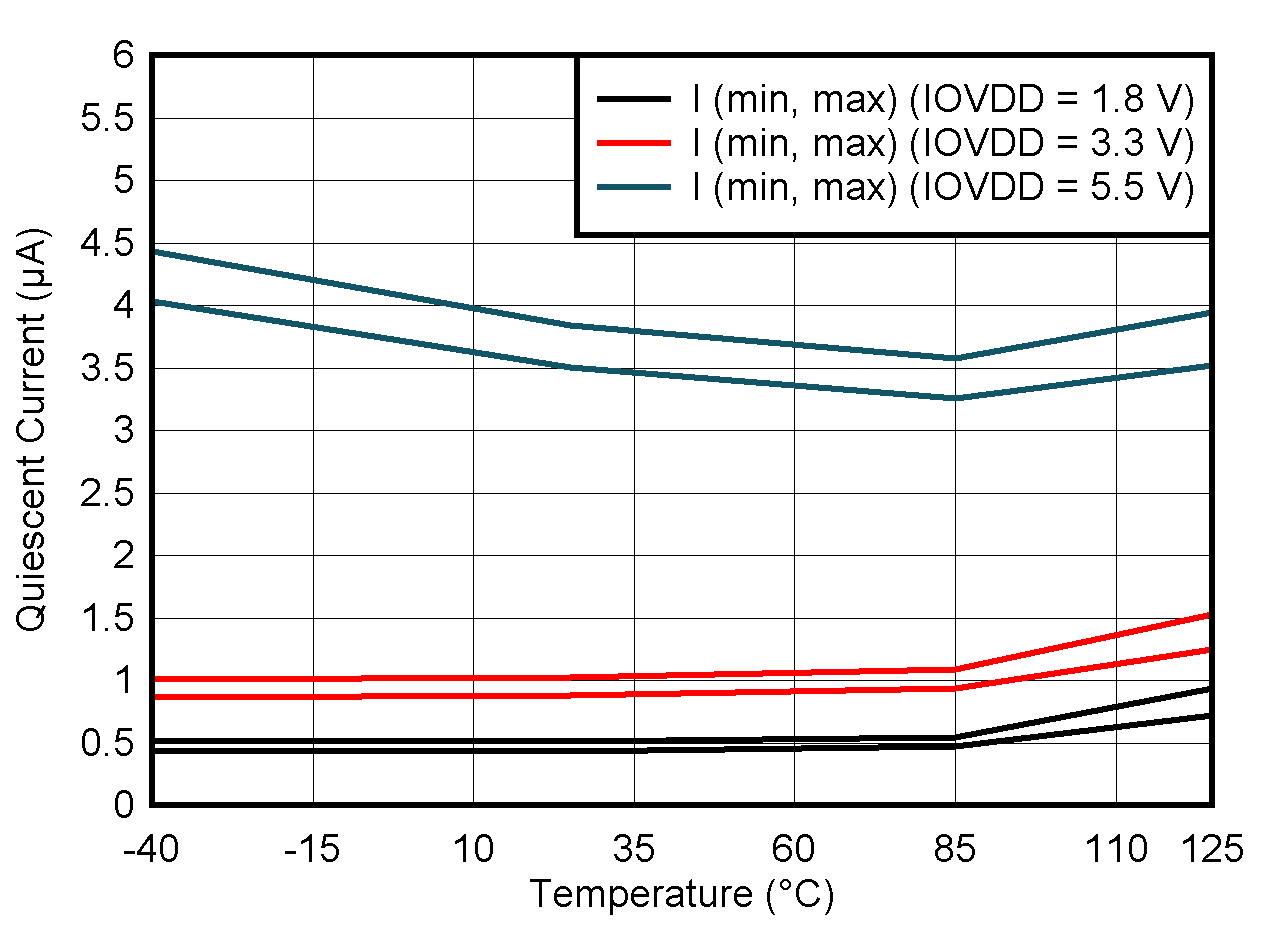
Typical Characteristics: Power Supply

at TA = 25°C, PVDD = IOVDD = 3.3 V, internal VREFIO, RLOAD = 50 kΩ to GND, CLOAD = 100 pF to GND, and digital inputs at IOVDD or GND (unless otherwise noted)

GUID-20221027-SS0I-NR3V-RDCG-GTKHNV7LFJZV-low.png
 
Figure 6-53 PVDD Supply Current vs Temperature
GUID-20221211-SS0I-JGMT-81FF-XKKP7FJ9FMCL-low.png
 
Figure 6-55 VDD Voltage vs Load Current
GUID-20221027-SS0I-NHG2-CXM5-69DD0XTTNQCZ-low.png
 
Figure 6-54 IOVDD Supply Current vs Temperature