SBASAF7C january   2022  – may 2023 AFE7906

PRODUCTION DATA  

  1.   1
  2. 1Features
  3. 2Applications
  4. 3Description
  5. 4Description (continued)
  6. 5Revision History
  7. 6Specifications
    1. 6.1  Absolute Maximum Ratings
    2. 6.2  ESD Ratings
    3. 6.3  Recommended Operating Conditions
    4. 6.4  Thermal Information
    5. 6.5  RF ADC Electrical Characteristics
    6. 6.6  PLL/VCO/Clock Electrical Characteristics
    7. 6.7  Digital Electrical Characteristics
    8. 6.8  Power Supply Electrical Characteristics
    9. 6.9  Timing Requirements
    10. 6.10 Switching Characteristics
    11. 6.11 Typical Characteristics
      1. 6.11.1 RX Typical Characteristics 30 MHz and 400 MHz
      2. 6.11.2 RX Typical Characteristics at 800MHz
      3. 6.11.3 RX Typical Characteristics 1.75GHz to 1.9GHz
      4. 6.11.4 RX Typical Characteristics 2.6GHz
      5. 6.11.5 RX Typical Characteristics 3.5GHz
      6. 6.11.6 RX Typical Characteristics 4.9GHz
      7. 6.11.7 RX Typical Characteristics 6.8GHz
      8. 6.11.8 PLL and Clock Typical Characteristics
  8. 7Device and Documentation Support
    1. 7.1 Receiving Notification of Documentation Updates
    2. 7.2 Support Resources
    3. 7.3 Trademarks
    4. 7.4 Electrostatic Discharge Caution
    5. 7.5 Glossary
  9. 8Mechanical, Packaging, and Orderable Information

Package Options

Mechanical Data (Package|Pins)
Thermal pad, mechanical data (Package|Pins)
Orderable Information

RX Typical Characteristics 2.6GHz

Typical values at TA = +25°C, ADC Sampling Rate = 2949.12 GHz. Default conditions: output sample rate = 491.52MSPS (decimate by 6), PLL clock mode with fREF = 491.52MHz, AIN = –3 dBFS, DSA setting = 4 dB.
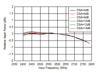
GUID-9A9CB8C1-69A8-47BE-91F0-30CEE66FDB4A-low.gif
With matching, normalized to power at 2.6 GHz for each DSA setting
Figure 6-111 RX Inband Gain Flatness, fIN = 2600 MHz
GUID-65E0D528-1BA8-4DA8-9EE6-7C08F628E8DA-low.gif
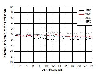
With 2.6 GHz matching
Integrated Phase Error = Phase(DSA Setting) – Phase(DSA Setting = 0)
Figure 6-113 RX Calibrated Integrated Phase Error vs DSA Setting at 2.6 GHz
GUID-D426693A-1B69-4F9A-A91B-B552E895C71C-low.gif
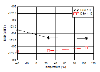
With 2.6 GHz matching, 12.5-MHz offset from tone
Figure 6-115 RX Noise Spectral Density vs Temperature at 2.6 GHz
GUID-F87CEDAF-4BA7-4579-A75E-2869E86CB0CD-low.gif
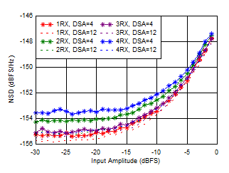
With 2.6 GHz matching, 12.5-MHz offset from tone
Figure 6-117 RX Noise Spectral Density vs Input Amplitude and Channel at 2.6 GHz
GUID-69131651-B9A4-4A1D-B847-0A34E2184E8B-low.gif
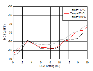
With 2.6 GHz matching, each tone –7 dBFS, tone spacing = 20 MHz
Figure 6-119 RX IMD3 vs DSA Setting and Temperature at 2.6 GHz
GUID-9AA5FC82-1344-4E4E-90B0-B2500A16FBD8-low.gif
With 2.6 GHz matching, tone spacing = 20 MHz, DSA = 12 dB
Figure 6-121 RX IMD3 vs Input Level and Temperature at 2.6 GHz
GUID-20210713-CA0I-MBFM-HZVD-1SSPZNFDVVZQ-low.png
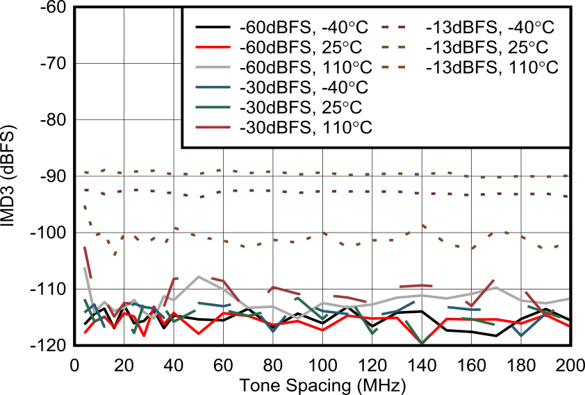
External clock mode
Figure 6-123 RX IMD3 vs Tone Spacing at 2.6 GHz (Ext. Clock)
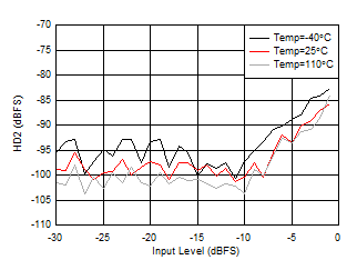
GUID-5B90B8F7-9F27-464B-8DB8-10E4883843DB-low.gif
With 2.6 GHz matching, DDC bypass mode (TI only mode for characterization)
Figure 6-125 RX HD2 vs Input Level and Temperature at 2.6 GHz
GUID-7DF79FD1-2C37-442C-A7F8-2DB4FAFBC666-low.gif
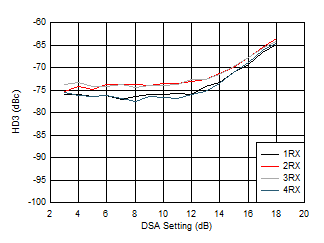
With 2.6 GHz matching, DDC bypass mode (TI only mode for characterization)
Figure 6-127 RX HD3 vs DSA Setting and Channel at 2.6 GHz
GUID-251903BA-C1BE-46FE-AE84-614E24E72B61-low.gif
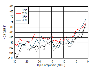
With 2.6 GHz matching, DDC bypass mode (TI only mode for characterization)
Figure 6-129 RX HD3 vs Input Level and Channel at 2.6 GHz
GUID-20210723-CA0I-WXSC-TGZ7-W4L2DFQSNJZL-low.svg
External clock mode
Figure 6-131 RX HD3 vs Input Level and Temperature at 2.6 GHz
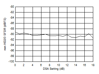
GUID-B9401131-6516-4CC1-917B-CD9CE3C5BA92-low.gif
With 2.6 GHz matching
Figure 6-133 RX Non-HD2/3 vs DSA Setting at 2.6 GHz
GUID-20220627-SS0I-ZKHS-HCGL-ZLTB7MTH9NTB-low.svg
With 2.6 GHz matching, –7 dBFS each tone, 20-MHz tone spacing, all supplies at MIN, TYP, or MAX recommended operating voltages
Figure 6-135 RX IMD3 vs Supply and Channel at 2.6 GHz
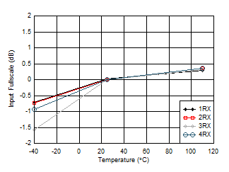
GUID-5F0BE996-585C-4C2A-A2AF-0449AECD4F11-low.gif
With 2.6 GHz matching, normalized to fullscale at 25°C for each channel
Figure 6-112 RX Input Fullscale vs Temperature and Channel at 2.6 GHz
GUID-95BE5240-6DBD-4252-B255-A5067B8318E7-low.gif
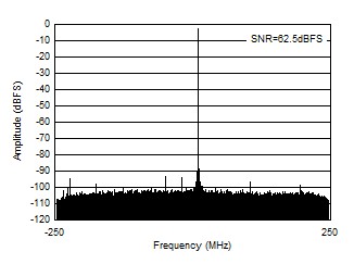
With 2.6 GHz matching, fIN = 2610 MHz, AIN= –3 dBFS
Figure 6-114 RX Output FFT at 2.6 GHz
GUID-4D9AAC29-0B16-40E4-8FC7-1ACB44A577AC-low.gif
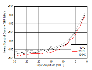
With 2.6 GHz matching, DSA Setting = 12 dB, 12.5-MHz offset from tone
Figure 6-116 RX Noise Spectral Density vs Input Amplitude and Temperature at 2.6 GHz
GUID-20210713-CA0I-VNVQ-BVPZ-1DJPWGTLJGFZ-low.svg
50-MHz offset from tone, external clock mode
Figure 6-118 RX Noise Spectral Density vs Input Amplitude at 2.61 GHz (Ext. Clock)
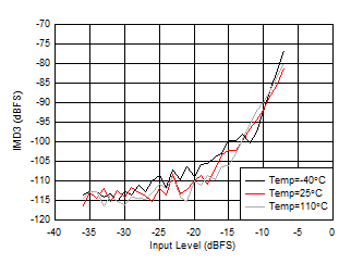
GUID-692099A6-9521-4982-B53A-047097808E51-low.gif
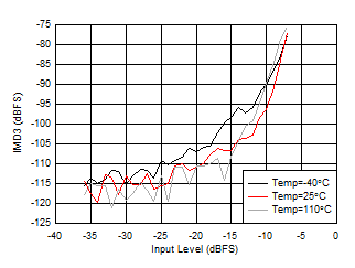
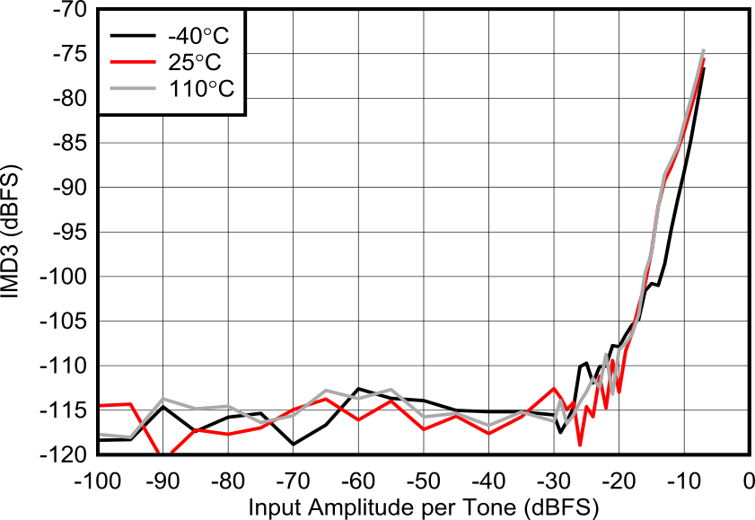
With 2.6 GHz matching, tone spacing = 20 MHz, DSA = 4 dB
Figure 6-120 RX IMD3 vs Input Level and Temperature at 2.6 GHz
GUID-20210713-CA0I-DWPX-QDZW-VMCBBGWM6HSQ-low.png
Tone spacing = 50 MHz, External clock mode
Figure 6-122 RX IMD3 vs Input Level at 2.6 GHz (Ext. Clock)
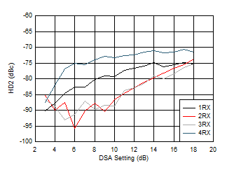
GUID-510692A9-A8A9-442B-A80A-FC5DED2E18B0-low.gif
With 2.6 GHz matching, DDC bypass mode (TI only mode for characterization)
Figure 6-124 RX HD2 vs DSA Setting and Channel at 2.6 GHz
GUID-20210723-CA0I-PXST-W2HM-NDTKXNGNCKJZ-low.svg
External clock mode
Figure 6-126 RX HD2 vs Input Level and Temperature at 2.6 GHz
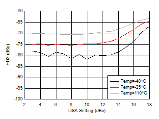
GUID-06F82D21-A375-4171-ACB8-1F40DD8C7744-low.gif
With 2.6 GHz matching, DDC bypass mode (TI only mode for characterization)
Figure 6-128 RX HD3 vs DSA Setting and Temperature at 2.6 GHz
GUID-1B74055D-29B4-4EF2-A275-F11D715EB9A3-low.gif
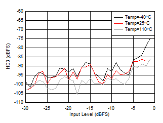
With 2.6 GHz matching, DDC bypass mode (TI only mode for characterization)
Figure 6-130 RX HD3 vs Input Level and Temperature at 2.6 GHz
GUID-3029F916-42B0-4A21-B87A-21C15AE500A9-low.gif
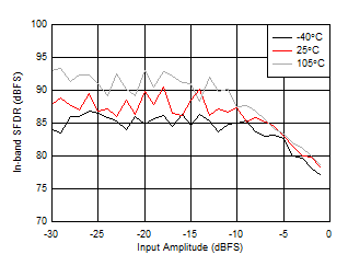
With 2.6 GHz matching, decimate by 4
Figure 6-132 RX In-Band SFDR (±300 MHz) vs Input Amplitude and Temperature at 2.6 GHz
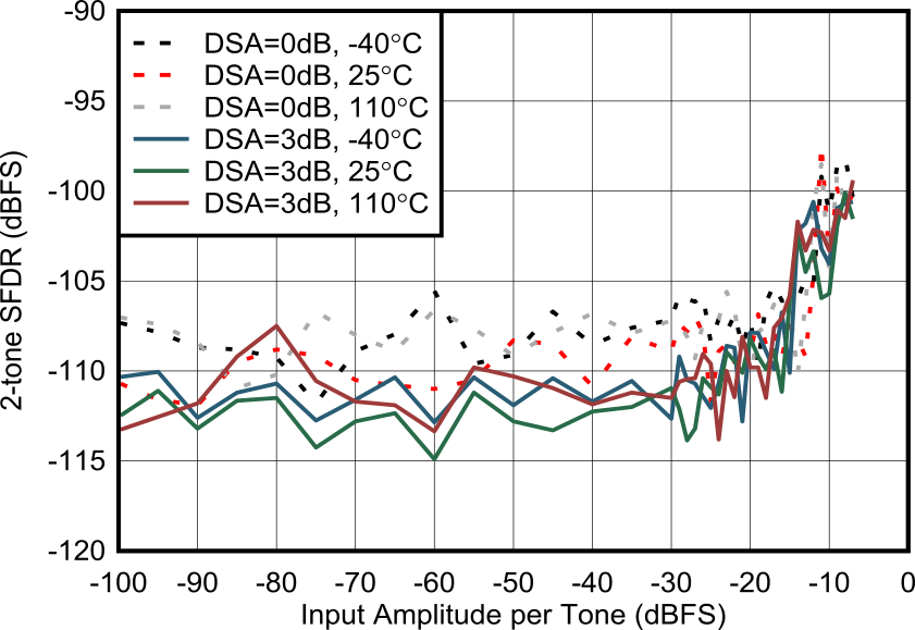
GUID-20210720-CA0I-BKVW-MQC1-LRP92Q1RWSBG-low.png
External clock mode, 50MHz tone spacing, excluding 3rd order distortion
Figure 6-134 RX 2-tone SFDR vs Input Amplitude at 2.6 GHz
GUID-20220627-SS0I-4ZNF-WVFB-CNF1P2WB3H6F-low.svg
With 2.6 GHz matching, 12.5-MHz offset, all supplies at MIN, TYP, or MAX recommended operating voltages
Figure 6-136 RX Noise Spectral Density vs Supply and Channel at 2.6 GHz