SBASAF7C january   2022  – may 2023 AFE7906

PRODUCTION DATA  

  1.   1
  2. 1Features
  3. 2Applications
  4. 3Description
  5. 4Description (continued)
  6. 5Revision History
  7. 6Specifications
    1. 6.1  Absolute Maximum Ratings
    2. 6.2  ESD Ratings
    3. 6.3  Recommended Operating Conditions
    4. 6.4  Thermal Information
    5. 6.5  RF ADC Electrical Characteristics
    6. 6.6  PLL/VCO/Clock Electrical Characteristics
    7. 6.7  Digital Electrical Characteristics
    8. 6.8  Power Supply Electrical Characteristics
    9. 6.9  Timing Requirements
    10. 6.10 Switching Characteristics
    11. 6.11 Typical Characteristics
      1. 6.11.1 RX Typical Characteristics 30 MHz and 400 MHz
      2. 6.11.2 RX Typical Characteristics at 800MHz
      3. 6.11.3 RX Typical Characteristics 1.75GHz to 1.9GHz
      4. 6.11.4 RX Typical Characteristics 2.6GHz
      5. 6.11.5 RX Typical Characteristics 3.5GHz
      6. 6.11.6 RX Typical Characteristics 4.9GHz
      7. 6.11.7 RX Typical Characteristics 6.8GHz
      8. 6.11.8 PLL and Clock Typical Characteristics
  8. 7Device and Documentation Support
    1. 7.1 Receiving Notification of Documentation Updates
    2. 7.2 Support Resources
    3. 7.3 Trademarks
    4. 7.4 Electrostatic Discharge Caution
    5. 7.5 Glossary
  9. 8Mechanical, Packaging, and Orderable Information

Package Options

Mechanical Data (Package|Pins)
Thermal pad, mechanical data (Package|Pins)
Orderable Information

RX Typical Characteristics 3.5GHz

Typical values at TA = +25°C, ADC Sampling Rate = 2949.12 GHz. Default conditions: output sample rate = 491.52MSPS (decimate by 6), PLL clock mode with fREF = 491.52MHz, AIN = –3 dBFS, DSA setting = 4 dB.
GUID-76EA8C01-7587-4E38-97BA-591E71E01D3E-low.gif
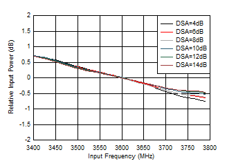
With 3.6 GHz matching, normalized to 3.6 GHz
Figure 6-137 RX In-Band Gain Flatness, fIN = 3600 MHz
GUID-C1D1FBB3-8132-4E00-AAC9-6FE23520B289-low.gif
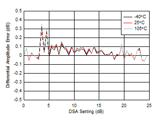
With 3.6 GHz matching
Differential Amplitude Error = PIN(DSA Setting – 1) – PIN(DSA Setting) + 1
Figure 6-139 RX Uncalibrated Differential Amplitude Error vs DSA Setting at 3.6 GHz
GUID-2AE563F1-F5B4-464A-9A8F-71A5EF428867-low.gif
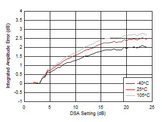
With 3.6 GHz matching
Integrated Amplitude Error = PIN(DSA Setting) – PIN(DSA Setting = 0) + (DSA Setting)
Figure 6-141 RX Uncalibrated Integrated Amplitude Error vs DSA Setting at 3.6 GHz
GUID-7FD1A100-F736-48C1-B9D9-4789A068672F-low.gif
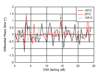
With 3.6 GHz matching
Differential Phase Error = PhaseIN(DSA Setting – 1) – PhaseIN(DSA Setting)
Figure 6-143 RX Uncalibrated Phase Error vs DSA Setting at 3.6 GHz
GUID-D607DFA2-5BC0-4AF1-9659-0C56797BE66F-low.gif
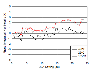
With 3.6 GHz matching
Integrated Phase Error = Phase(DSA Setting) – Phase(DSA Setting = 0)
Figure 6-145 RX Uncalibrated Integrated Phase Error vs DSA Setting at 3.6 GHz
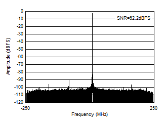
GUID-491F723F-2696-42E6-A2E4-AC5890D36033-low.gif
With 3.6 GHz matching , fIN = 3610 MHz, AIN = –3 dBFS
Figure 6-147 RX Output FFT at 3.6 GHz
GUID-F7E6092E-B634-4A14-B1BE-5399FC861650-low.gif
With 3.5 GHz matching, 20-MHz tone spacing
Figure 6-149 RX IMD3 vs Input Level and Temperature at 3.6 GHz
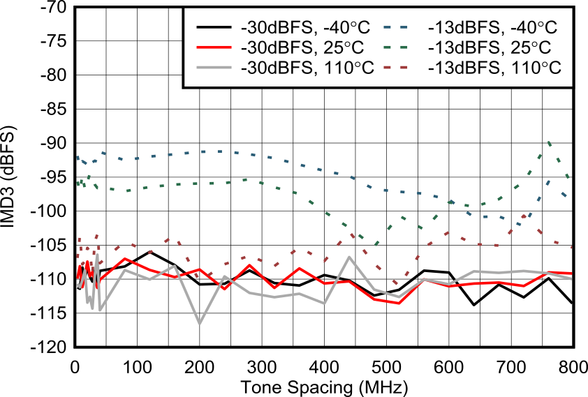
GUID-20210713-CA0I-KHSL-6LJV-NRSX32DJWMF5-low.png
External clock mode, 2x Decimation
Figure 6-151 RX IMD3 vs Tone Spacing at 3.76GHz
GUID-F232A7CB-9D5C-445B-98C9-0D9D1D6752AD-low.gif
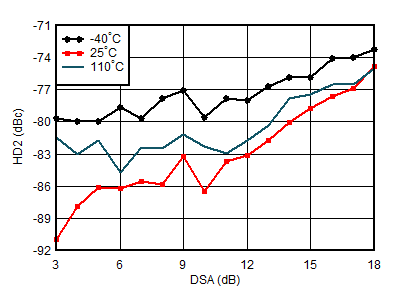
With 3.5 GHz matching, DDC bypass mode (TI only mode for characterization)
Figure 6-153 RX HD2 vs DSA Setting and Temperature at 3.6 GHz
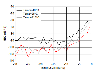
GUID-3CE19B63-2A7D-4FF9-A03E-099E090D84F0-low.gif
With 3.5 GHz matching, DDC bypass mode (TI only mode for characterization)
Figure 6-155 RX HD2 vs Input Level and Temperature at 3.6 GHz
GUID-20210713-CA0I-8HGD-BTVN-6FLSVQDQF13N-low.svg
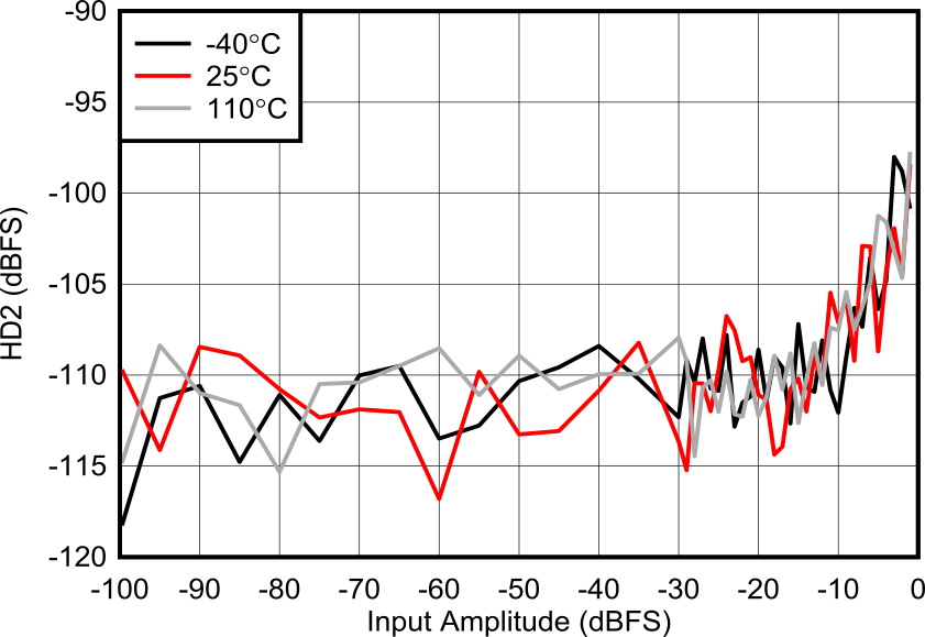
External clock mode, 25°C, 2x Decimation
Figure 6-157 RX HD2 vs Input Level
GUID-309DB605-854C-4AF1-B823-CD18850455E1-low.gif
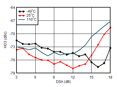
With 3.5 GHz matching, DDC bypass mode (TI only mode for characterization)
Figure 6-159 RX HD3 vs DSA Setting and Temperature at 3.6 GHz
GUID-959F80ED-9240-4335-AE3C-7FEA5C5EA331-low.gif
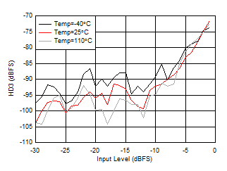
With 3.5 GHz matching, DDC bypass mode (TI only mode for characterization)
Figure 6-161 RX HD3 vs Input Level and Temperature at 3.6 GHz
GUID-20210713-CA0I-6PXN-QDCT-RMCCD2PP00BC-low.png
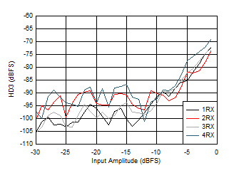
External clock mode, 25°C, 2x Decimation
Figure 6-163 RX HD3 vs Input Level
GUID-20210713-CA0I-0KGT-WB5C-W4DLLFHBQ2DM-low.png
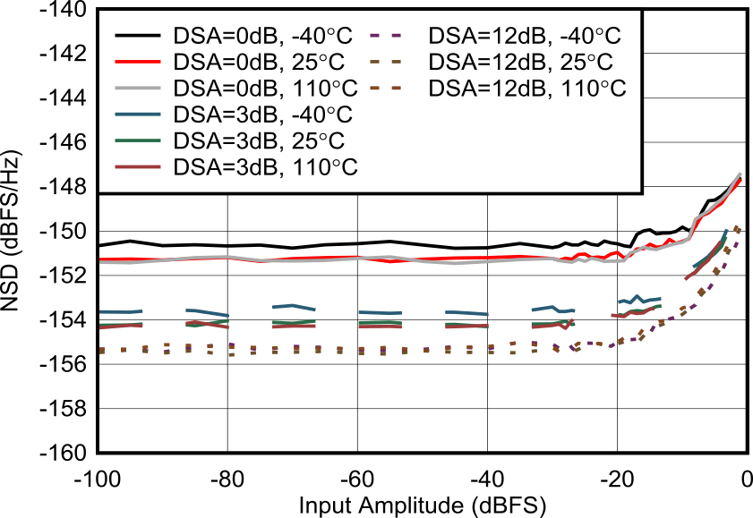
External clock mode, 25°C, 2x Decimation
Figure 6-165 RX Noise Spectral Density vs Input Level at 3.76GHz
GUID-3EE48593-44FE-4D2E-A5D9-789C7A49E5FF-low.gif
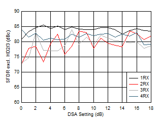
With 3.5 GHz matching
Figure 6-167 RX SFDR Excluding HD2/3 vs DSA Setting and Channel at 3.6 GHz
GUID-20210720-CA0I-M1HB-2P3W-4PLPQWPB2RK3-low.png
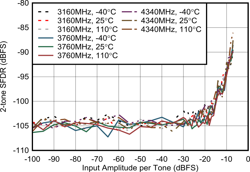
External clock mode, 20MHz tone spacing, excluding 3rd order distortion
Figure 6-169 RX 2-tone SFDR vs Input Amplitude and Frequency at 3.7 GHz
GUID-20220627-SS0I-HDCW-MGVB-SPS9H9K9MTD8-low.svg
With 3.6 GHz matching, –7 dBFS each tone, 20-MHz tone spacing, all supplies at MIN, TYP, or MAX recommended operating voltages
Figure 6-171 RX IMD5 vs Supply Voltage and Channel at 3.6 GHz
GUID-DE756DF5-9910-4F4B-AC33-804AA135735B-low.gif
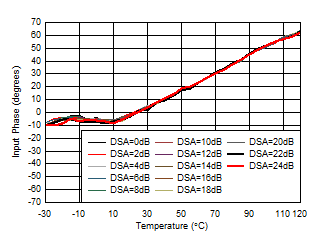
With 3.6 GHz matching, normalized to phase at 25°C
Figure 6-138 RX Input Phase vs Temperature at 3.6 GHz
GUID-601C686C-DC69-46B4-9C08-E0B43B0EC7EB-low.gif
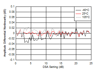
With 3.6 GHz matching
Differential Amplitude Error = PIN(DSA Setting – 1) – PIN(DSA Setting) + 1
Figure 6-140 RX Calibrated Differential Amplitude Error vs DSA Setting at 3.6 GHz
GUID-286BD3D8-C1C6-43EF-9F7A-F7EE08011C51-low.gif
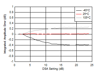
With 3.6 GHz matching
Integrated Amplitude Error = PIN(DSA Setting) – PIN(DSA Setting = 0) + (DSA Setting)
Figure 6-142 RX Calibrated Integrated Amplitude Error vs DSA Setting at 3.6 GHz
GUID-7378D37E-7B6D-47A0-A172-1E75B97E1FB8-low.gif
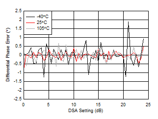
With 3.6 GHz matching
Differential Phase Error = PhaseIN(DSA Setting – 1) – PhaseIN(DSA Setting)
Figure 6-144 RX Calibrated Differential Phase Error vs DSA Setting at 3.6 GHz
GUID-82EA5C11-8B01-4821-A4DC-AB4AA6520410-low.gif
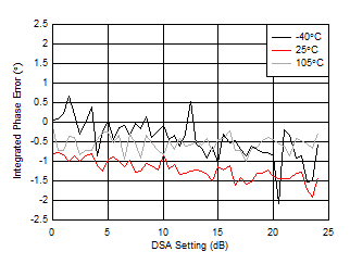
With 3.6 GHz matching
Integrated Phase Error = Phase(DSA Setting) – Phase(DSA Setting = 0)
Figure 6-146 RX Calibrated Integrated Phase Error vs DSA Setting at 3.6 GHz
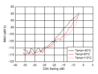
GUID-253AD12B-86DB-40BD-A1A1-0EE7508BEEE5-low.gif
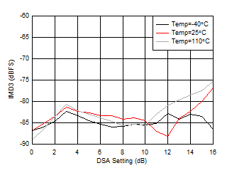
With 3.5 GHz matching, each tone at –7 dBFS, 20-MHz tone spacing
Figure 6-148 RX IMD3 vs DSA Setting and Temperature at 3.6 GHz
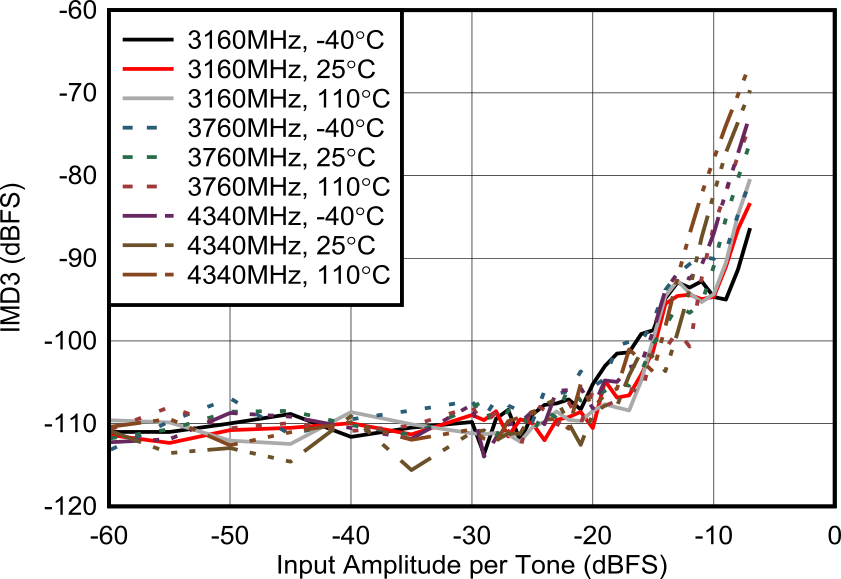
GUID-20210709-CA0I-9TPX-ZVTK-G1FCG78PDBSW-low.png
External clock mode, 20-MHz tone spacing, 2x Decimation
Figure 6-150 RX IMD3 vs Input Level
GUID-80A257B1-9969-4E57-862A-5A0C2B7FFBB6-low.gif
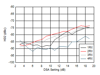
With 3.5 GHz matching, DDC bypass mode (TI only mode for characterization)
Figure 6-152 RX HD2 vs DSA Setting and Channel at 3.6 GHz
GUID-3745D214-4491-434B-9ACD-0D81F3D6F2FF-low.gif
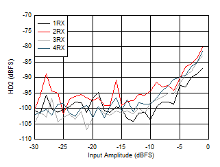
With 3.5 GHz matching, DDC bypass mode (TI only mode for characterization)
Figure 6-154 RX HD2 vs Input Level and Channel at 3.6 GHz
GUID-20210713-CA0I-6N7X-FQQC-KTM19LPJVDFJ-low.png
External clock mode, 2x Decimation
Figure 6-156 RX HD2 vs Input Level at 3.76 GHz
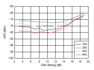
GUID-F5634162-46F5-4760-9B3F-6DDA0AF689CE-low.gif
With 3.5 GHz matching, DDC bypass mode (TI only mode for characterization)
Figure 6-158 RX HD3 vs DSA Setting and Channel at 3.6 GHz
GUID-0950FEA0-0C71-4390-9296-89F9DCE46DE3-low.gif
With 3.5 GHz matching, DDC bypass mode (TI only mode for characterization)
Figure 6-160 RX HD3 vs Input Level and Channel at 3.6 GHz
GUID-20210713-CA0I-RSHK-SQZK-N9JRZHXBNNWN-low.svg
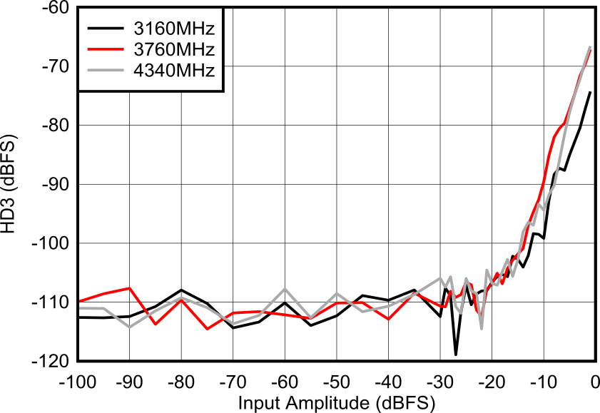
External clock mode, 2x Decimation
Figure 6-162 RX HD3 vs Input Level at 3.76GHz
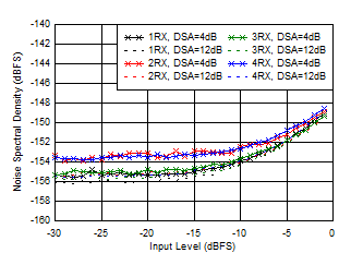
GUID-6003AA8B-B401-4332-9743-AD1717067278-low.gif
With 3.5 GHz matching, 12.5-MHz offset from tone
Figure 6-164 RX Noise Spectral Density vs Input Level and DSA Setting at 3.6 GHz
GUID-BEEDCA85-4E6D-4FAF-A2CD-364504BF1122-low.gif
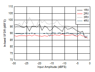
With 3.5 GHz matching
Figure 6-166 RX In-Band SFDR (±200 MHz) vs Input Level and Channel at 3.6 GHz
GUID-20210720-CA0I-DPRZ-L5NT-M6768D6NVK7R-low.svg
External clock mode, 20MHz tone spacing, excluding 3rd order distortion
Figure 6-168 RX 2-tone SFDR vs Input Amplitude and DSA Setting at 3.7 GHz
GUID-20220627-SS0I-P9TF-G3FS-07CJNN7F1FDJ-low.svg
With 3.6 GHz matching, –7 dBFS each tone, 20-MHz tone spacing, all supplies at MIN, TYP, or MAX recommended operating voltages
Figure 6-170 RX IMD3 vs Supply Voltage and Channel at 3.6 GHz
GUID-20220627-SS0I-BGTM-L1LD-0L3PDM243VVZ-low.svg
With 3.6 GHz matching, tone at –20 dBFS, 12.5-MHz offset frequency, all supplies at MIN, TYP, or MAX recommended operating voltages
Figure 6-172 RX Noise Spectral Density vs Supply Voltage and Channel at 3.6 GHz