SLASF44A May   2023  – June 2024 AFE78201 , AFE88201

PRODUCTION DATA  

  1.   1
  2. Features
  3. Applications
  4. Description
  5. Pin Configuration and Functions
  6. Specifications
    1. 5.1  Absolute Maximum Ratings
    2. 5.2  ESD Ratings
    3. 5.3  Recommended Operating Conditions
    4. 5.4  Thermal Information
    5. 5.5  Electrical Characteristics
    6. 5.6  Timing Requirements
    7. 5.7  Timing Diagrams
    8. 5.8  Typical Characteristics: VOUT DAC
    9. 5.9  Typical Characteristics: ADC
    10. 5.10 Typical Characteristics: Reference
    11. 5.11 Typical Characteristics: Power Supply
  7. Detailed Description
    1. 6.1 Overview
    2. 6.2 Functional Block Diagram
    3. 6.3 Feature Description
      1. 6.3.1  Digital-to-Analog Converter (DAC) Overview
        1. 6.3.1.1 DAC Resistor String
        2. 6.3.1.2 DAC Buffer Amplifier
        3. 6.3.1.3 DAC Transfer Function
        4. 6.3.1.4 DAC Gain and Offset Calibration
        5. 6.3.1.5 Programmable Slew Rate
        6. 6.3.1.6 DAC Register Structure and CLEAR State
      2. 6.3.2  Analog-to-Digital Converter (ADC) Overview
        1. 6.3.2.1 ADC Operation
        2. 6.3.2.2 ADC Custom Channel Sequencer
        3. 6.3.2.3 ADC Synchronization
        4. 6.3.2.4 ADC Offset Calibration
        5. 6.3.2.5 External Monitoring Inputs
        6. 6.3.2.6 Temperature Sensor
        7. 6.3.2.7 Self-Diagnostic Multiplexer
        8. 6.3.2.8 ADC Bypass
      3. 6.3.3  Programmable Out-of-Range Alarms
        1. 6.3.3.1 Alarm-Based Interrupts
        2. 6.3.3.2 Alarm Action Configuration Register
        3. 6.3.3.3 Alarm Voltage Generator
        4. 6.3.3.4 Temperature Sensor Alarm Function
        5. 6.3.3.5 Internal Reference Alarm Function
        6. 6.3.3.6 ADC Alarm Function
        7. 6.3.3.7 Fault Detection
      4. 6.3.4  IRQ
      5. 6.3.5  Internal Reference
      6. 6.3.6  Integrated Precision Oscillator
      7. 6.3.7  Precision Oscillator Diagnostics
      8. 6.3.8  One-Time Programmable (OTP) Memory
      9. 6.3.9  GPIO
      10. 6.3.10 Timer
      11. 6.3.11 Unique Chip Identifier (ID)
      12. 6.3.12 Scratch Pad Register
    4. 6.4 Device Functional Modes
      1. 6.4.1 Register Built-In Self-Test (RBIST)
      2. 6.4.2 DAC Power-Down Mode
      3. 6.4.3 Reset
    5. 6.5 Programming
      1. 6.5.1 Communication Setup
        1. 6.5.1.1 SPI Mode
        2. 6.5.1.2 UART Mode
      2. 6.5.2 GPIO Programming
      3. 6.5.3 Serial Peripheral Interface (SPI)
        1. 6.5.3.1 SPI Frame Definition
        2. 6.5.3.2 SPI Read and Write
        3. 6.5.3.3 Frame Error Checking
        4. 6.5.3.4 Synchronization
      4. 6.5.4 UART Interface
        1. 6.5.4.1 UART Break Mode (UBM)
      5. 6.5.5 Status Bits
      6. 6.5.6 Watchdog Timer
  8. Register Maps
    1. 7.1 AFEx8201 Registers
  9. Application and Implementation
    1. 8.1 Application Information
      1. 8.1.1 Multichannel Configuration
    2. 8.2 Typical Application
      1. 8.2.1 Analog Output Module
        1. 8.2.1.1 Design Requirements
        2. 8.2.1.2 Detailed Design Procedure
          1. 8.2.1.2.1 XTR305
            1. 8.2.1.2.1.1 Current-Output Mode
            2. 8.2.1.2.1.2 Voltage Output Mode
            3. 8.2.1.2.1.3 Diagnostic Features
        3. 8.2.1.3 Application Curves
    3. 8.3 Initialization Setup
    4. 8.4 Power Supply Recommendations
    5. 8.5 Layout
      1. 8.5.1 Layout Guidelines
      2. 8.5.2 Layout Example
  10. Device and Documentation Support
    1. 9.1 Documentation Support
      1. 9.1.1 Related Documentation
    2. 9.2 Receiving Notification of Documentation Updates
    3. 9.3 Support Resources
    4. 9.4 Trademarks
    5. 9.5 Electrostatic Discharge Caution
    6. 9.6 Glossary
  11. 10Revision History
  12. 11Mechanical, Packaging, and Orderable Information

Package Options

Refer to the PDF data sheet for device specific package drawings

Mechanical Data (Package|Pins)
  • RRU|24
Thermal pad, mechanical data (Package|Pins)
Orderable Information

Typical Characteristics: VOUT DAC

at TA = 25°C, PVDD = 2.7 V, IOVDD = 1.8 V, external or internal VREFIO = 1.25 V, RLOAD = 50 kΩ to GND, CLOAD = 100 pF to GND, and digital inputs at IOVDD or GND (unless otherwise noted)
AFE78201 AFE88201 DAC
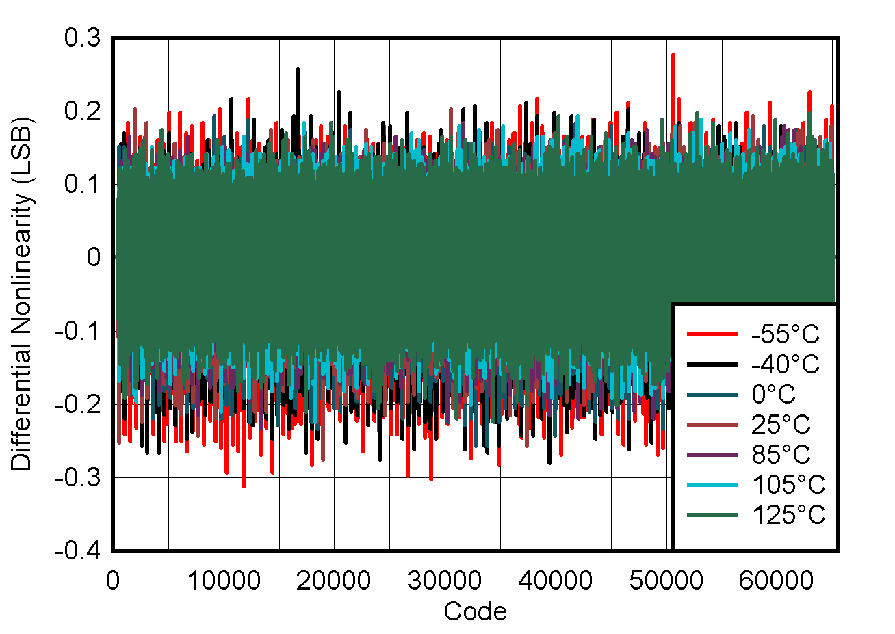
                        DNL vs Digital Input Code
 
Figure 5-3 DAC DNL vs Digital Input Code
AFE78201 AFE88201 DAC
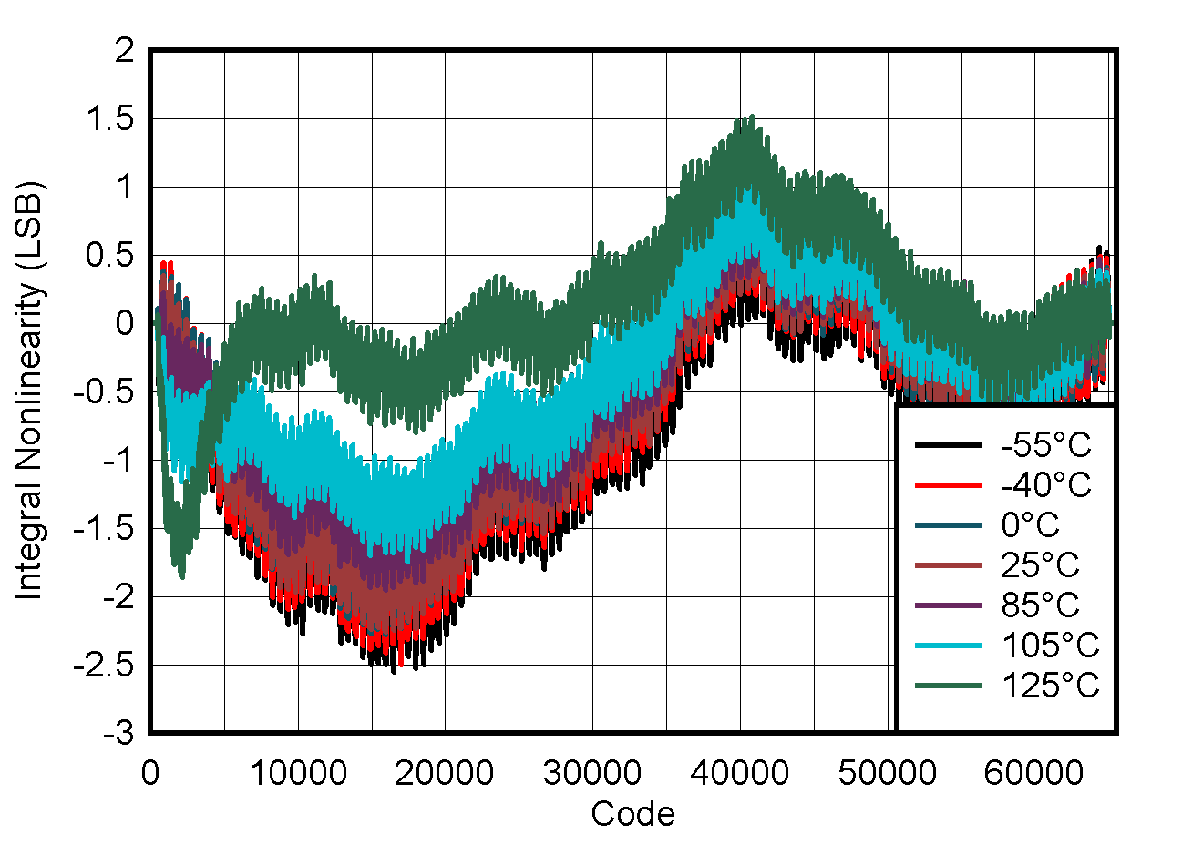
                        INL vs Digital Input Code
 
Figure 5-5 DAC INL vs Digital Input Code
AFE78201 AFE88201 DAC
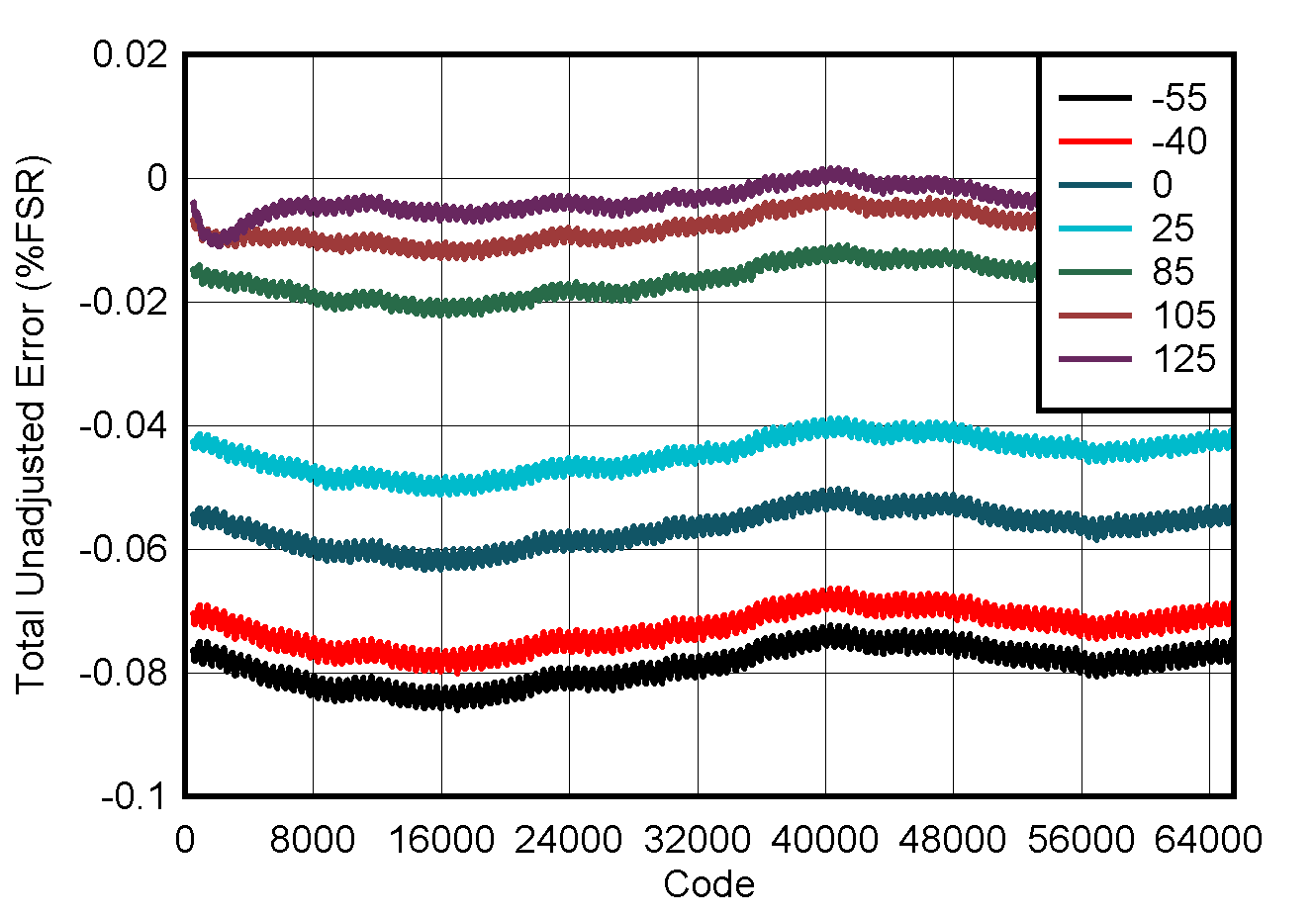
                        TUE vs Digital Input Code
 
Figure 5-7 DAC TUE vs Digital Input Code
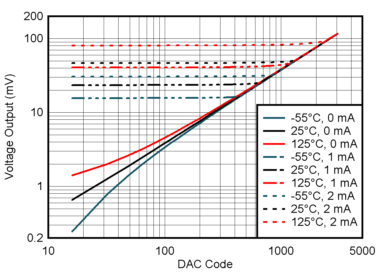
AFE78201 AFE88201 Zero-code Impedance
 
Figure 5-9 Zero-code Impedance
AFE78201 AFE88201 DAC
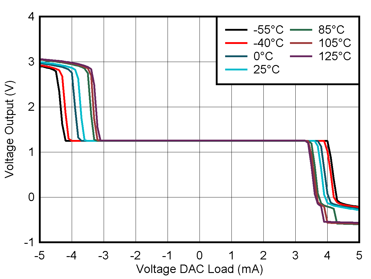
                        Source and Sink Current Capability
DAC at midcode
Figure 5-11 DAC Source and Sink Current Capability
AFE78201 AFE88201 DAC
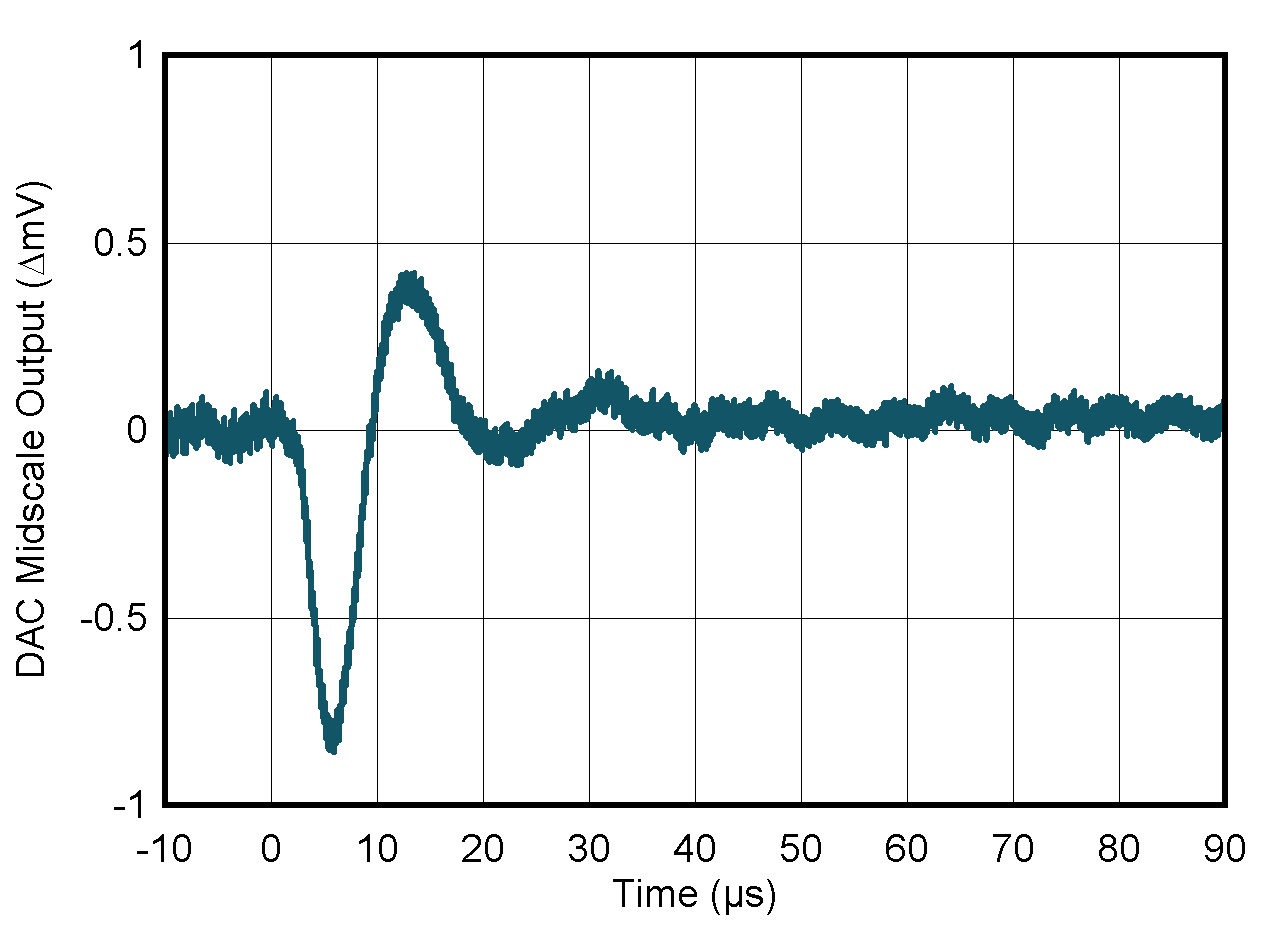
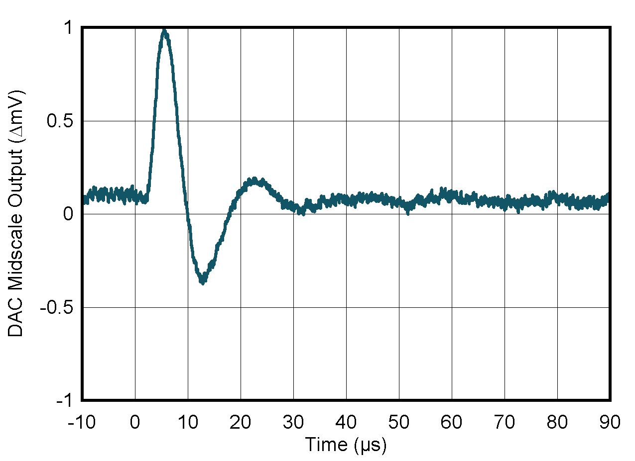
                        Glitch Impulse Rising Edge
PVDD = 5.5 V
Figure 5-13 DAC Glitch Impulse Rising Edge
AFE78201 AFE88201 DAC
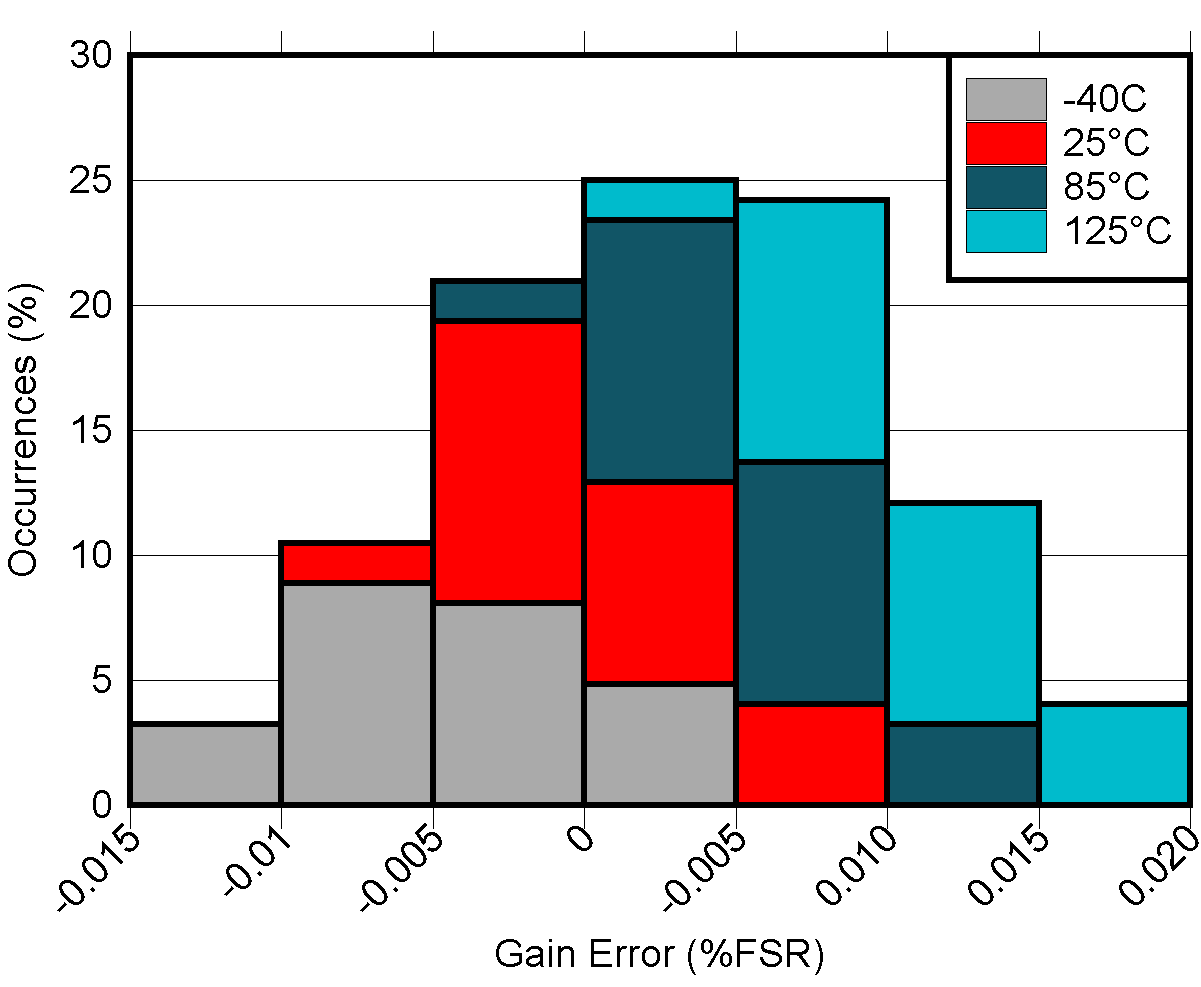
                        Gain Error vs TemperatureFigure 5-15 DAC Gain Error vs Temperature
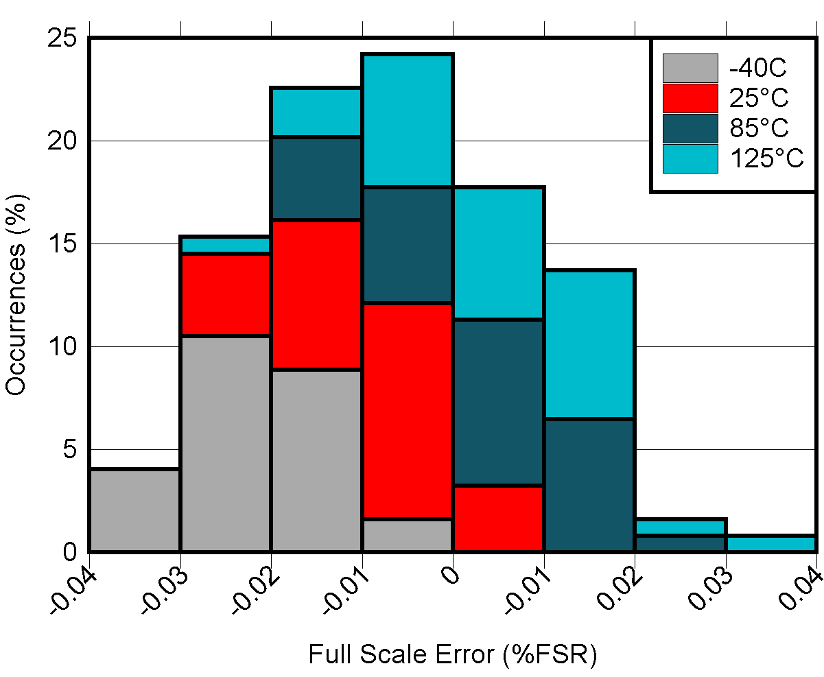
AFE78201 AFE88201 DAC
                        Full Scale Error vs TemperatureFigure 5-17 DAC Full Scale Error vs Temperature
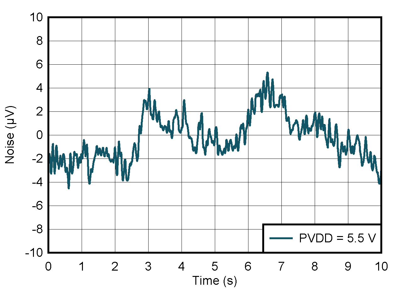
AFE78201 AFE88201 DAC
                        Output Noise, 0.1 Hz to 10 Hz
DAC at midcode PVDD = 5.5 V
Figure 5-19 DAC Output Noise, 0.1 Hz to 10 Hz
AFE78201 AFE88201 DAC
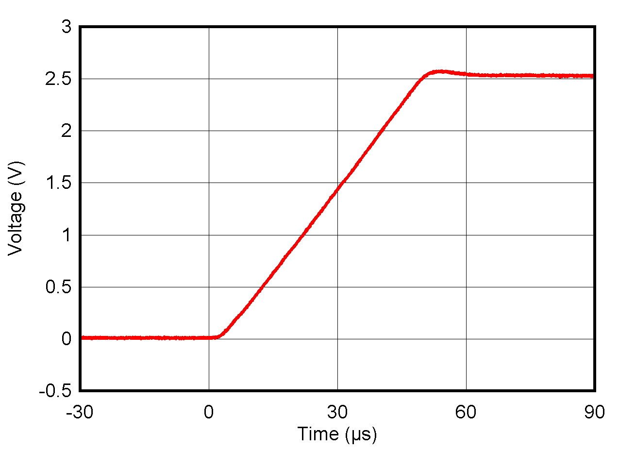
                        Rising Settling Time
 
Figure 5-21 DAC Rising Settling Time
AFE78201 AFE88201 DAC
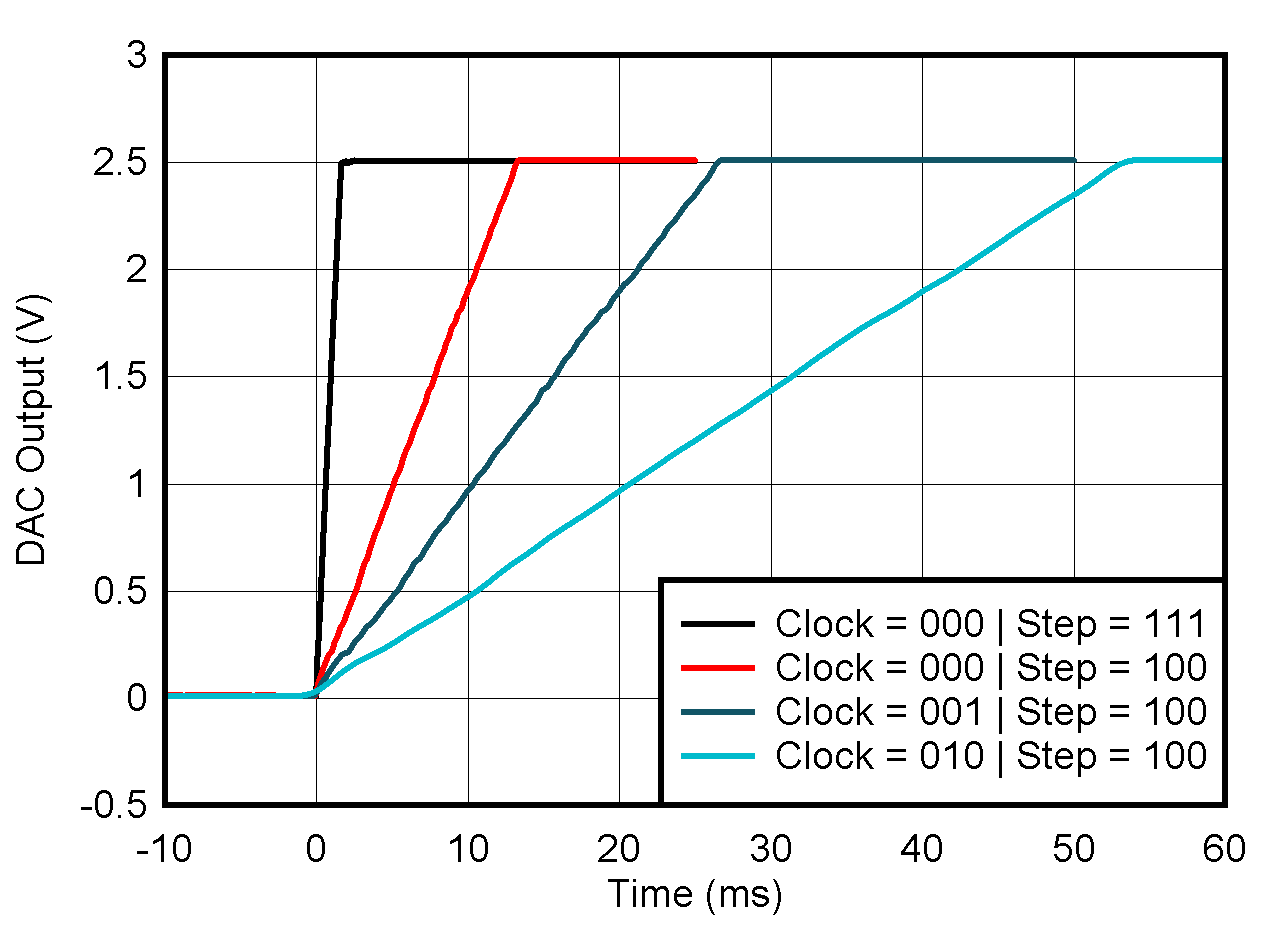
                        Settling Time With Linear Slew Rate Control
 
Figure 5-23 DAC Settling Time With Linear Slew Rate Control
AFE78201 AFE88201 DAC
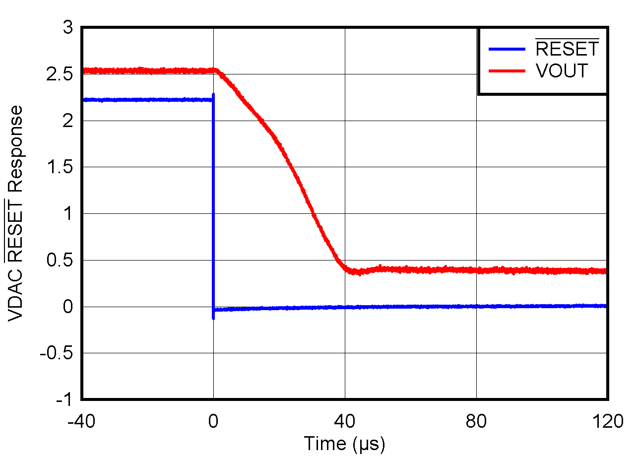
                            RESET Response
 
Figure 5-25 DAC RESET Response
AFE78201 AFE88201 DAC
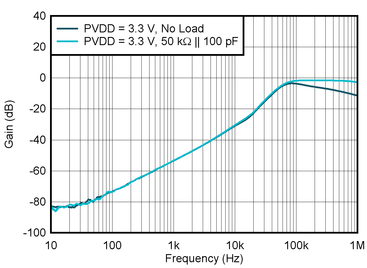
                        AC PSRR vs Frequency
Internal reference
Figure 5-27 DAC AC PSRR vs Frequency
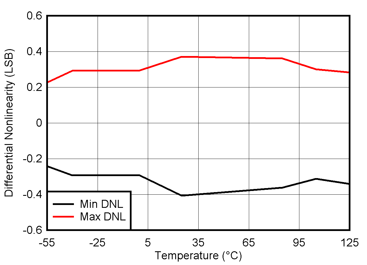
AFE78201 AFE88201 MIN
                        and MAX DAC DNL Range vs Temperature
 
Figure 5-4 MIN and MAX DAC DNL Range vs Temperature
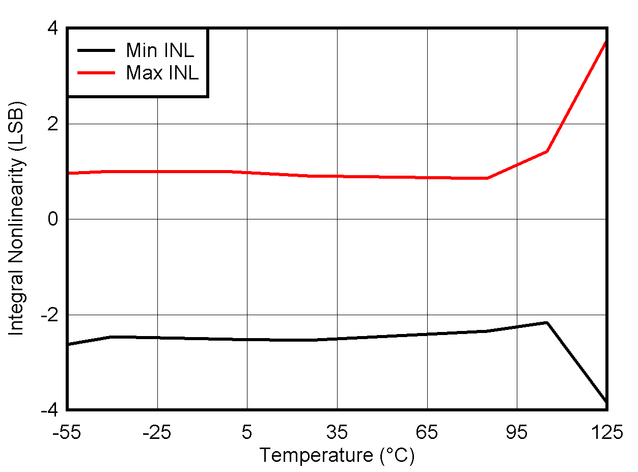
AFE78201 AFE88201 MIN
                        and MAX DAC INL Range vs Temperature
 
Figure 5-6 MIN and MAX DAC INL Range vs Temperature
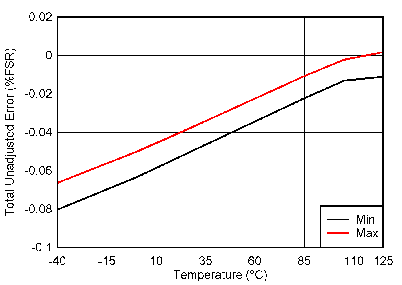
AFE78201 AFE88201 MIN
                        and MAX DAC TUE vs Temperature
 
Figure 5-8 MIN and MAX DAC TUE vs Temperature
AFE78201 AFE88201 DAC
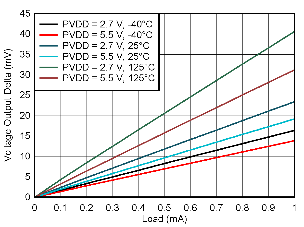
                        Footroom Over Temperature and Load
 
Figure 5-10 DAC Footroom Over Temperature and Load
AFE78201 AFE88201 DAC
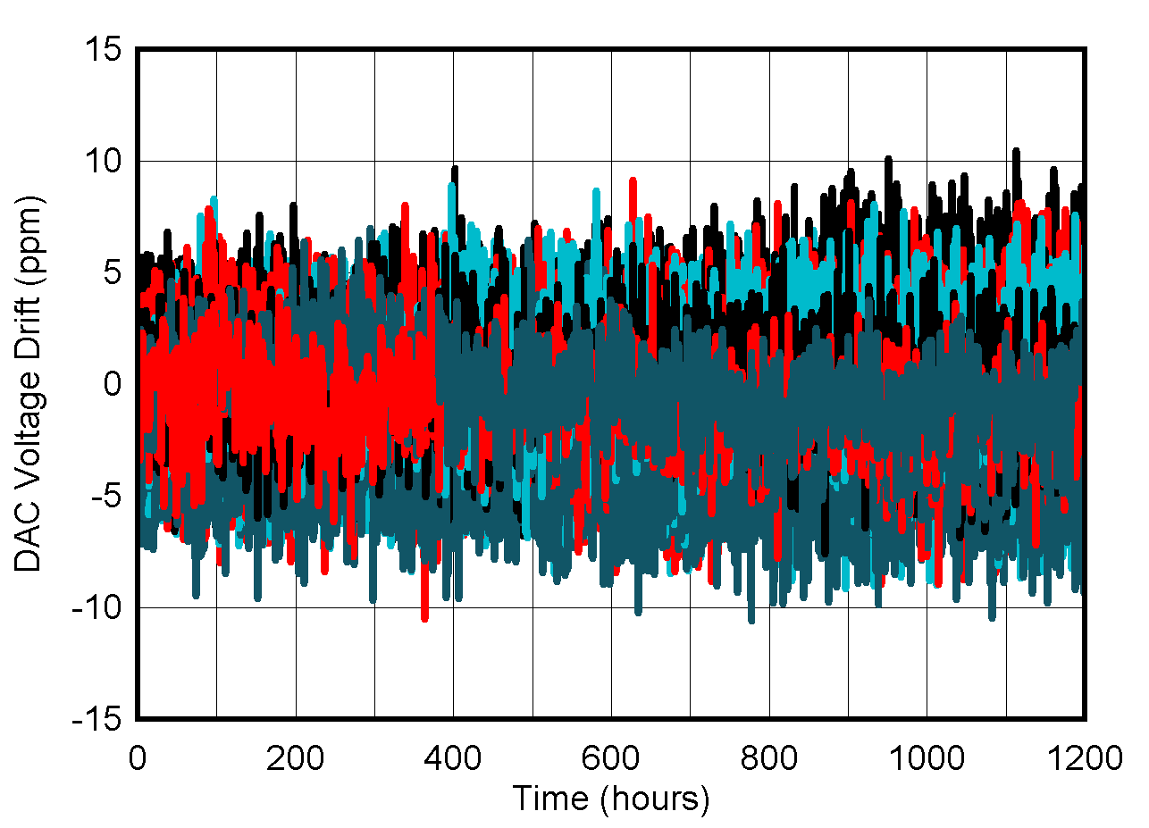
                        Output Voltage Long-Term Stability
Ideal reference
Figure 5-12 DAC Output Voltage Long-Term Stability
AFE78201 AFE88201 DAC
                        Glitch Impulse Falling Edge
PVDD = 5.5 V
Figure 5-14 DAC Glitch Impulse Falling Edge
AFE78201 AFE88201 DAC
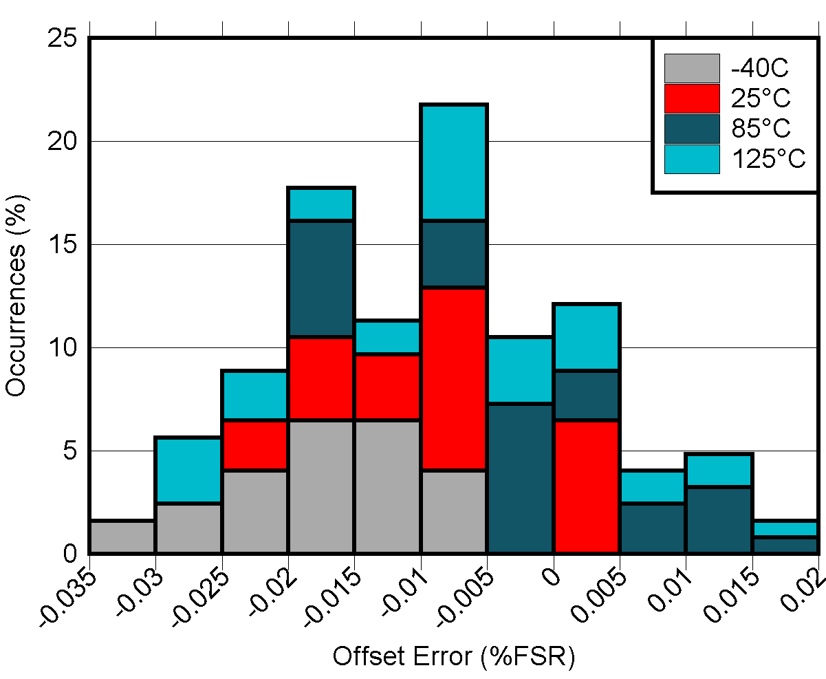
                        Offset Error vs TemperatureFigure 5-16 DAC Offset Error vs Temperature
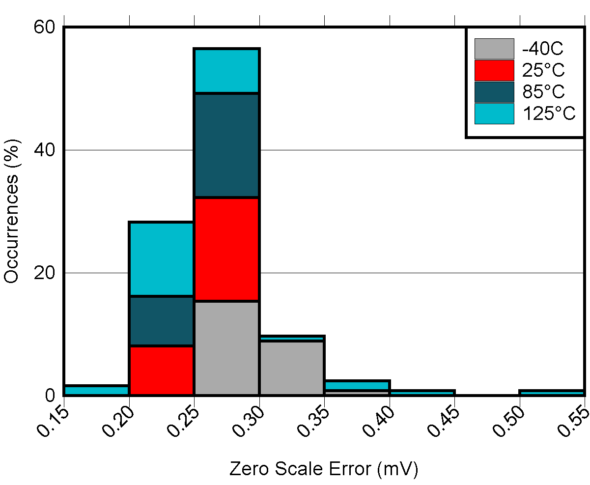
AFE78201 AFE88201 DAC
                        Zero Scale Error vs TemperatureFigure 5-18 DAC Zero Scale Error vs Temperature
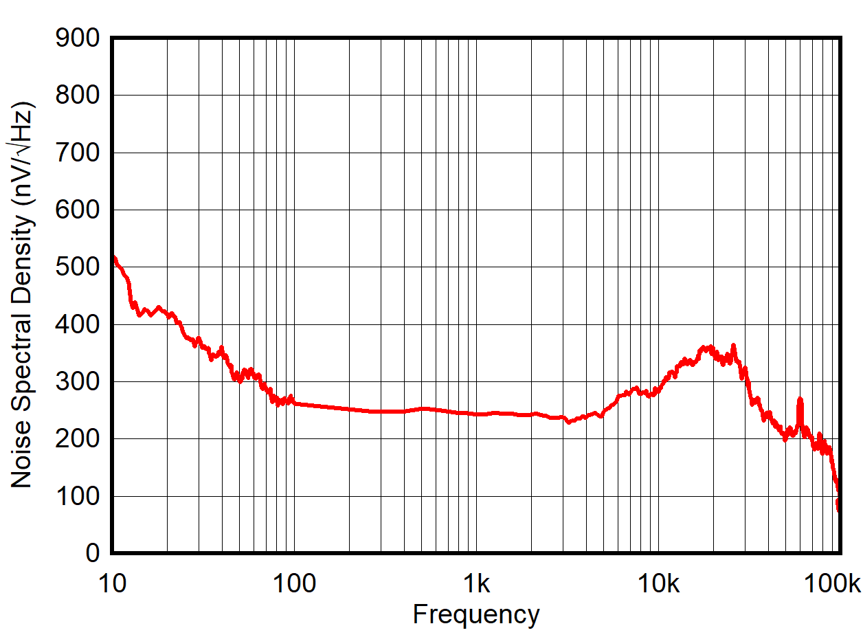
AFE78201 AFE88201 DAC
                        Output Noise Density vs Frequency
DAC at midcode PVDD = 5.5 V
Figure 5-20 DAC Output Noise Density vs Frequency
AFE78201 AFE88201 DAC
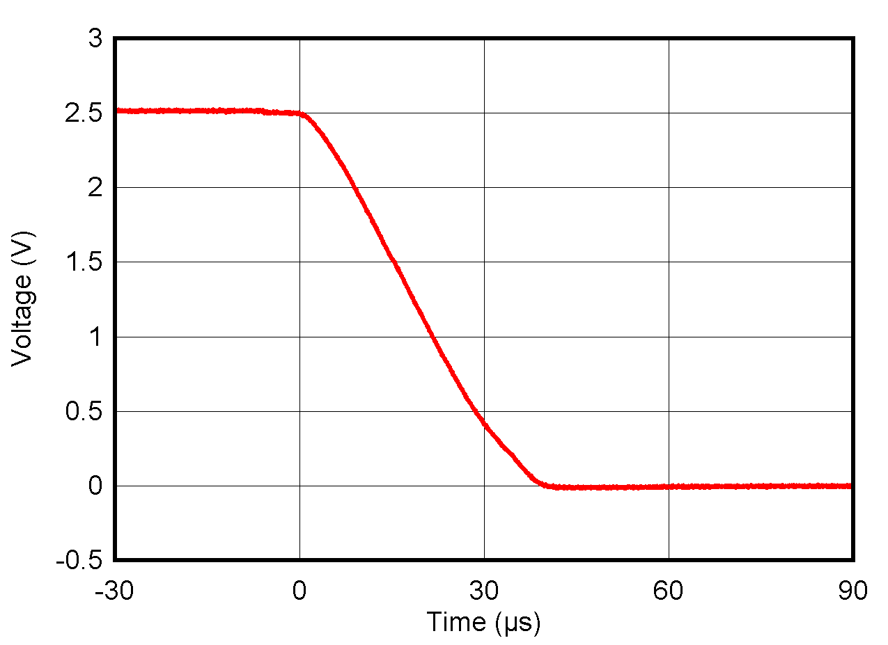
                        Falling Settling Time
 
Figure 5-22 DAC Falling Settling Time
AFE78201 AFE88201 DAC
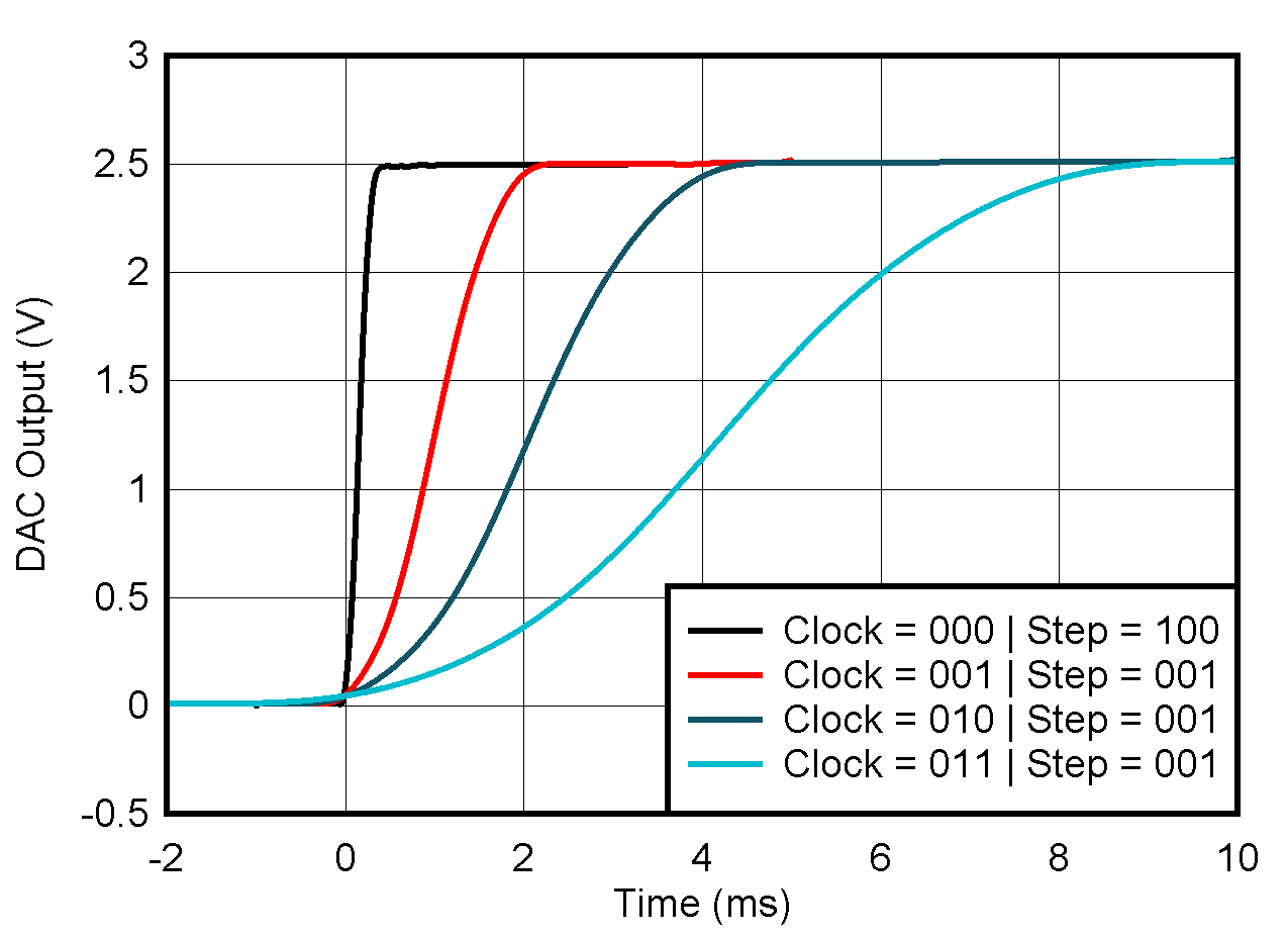
                        Settling Time With Sinusoidal Slew Rate Control
 
Figure 5-24 DAC Settling Time With Sinusoidal Slew Rate Control
AFE78201 AFE88201 DAC
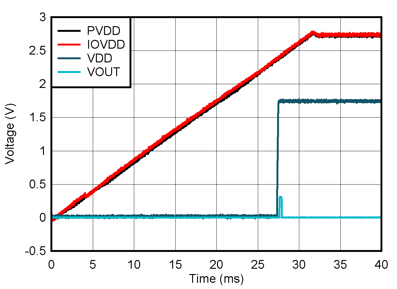
                        Supply Power On, PVDD = 2.7 V
 
Figure 5-26 DAC Supply Power On, PVDD = 2.7 V