SPRSP58B june 2022 – june 2023 AM620-Q1 , AM623 , AM625 , AM625-Q1
PRODUCTION DATA
- 1
- 1 Features
- 2 Applications
- 3 Description
- 4 Revision History
- 5 Device Comparison
-
6 Terminal Configuration and Functions
- 6.1 Pin Diagrams
- 6.2 Pin Attributes
- 6.3
Signal Descriptions
- 15
- 6.3.1 CPSW3G
- 6.3.2 CPTS
- 6.3.3 CSI-2
- 6.3.4 DDRSS
- 6.3.5 DSS
- 6.3.6 ECAP
- 6.3.7 Emulation and Debug
- 6.3.8 EPWM
- 6.3.9 EQEP
- 6.3.10 GPIO
- 6.3.11 GPMC
- 6.3.12 I2C
- 6.3.13 MCAN
- 6.3.14 MCASP
- 6.3.15 MCSPI
- 6.3.16 MDIO
- 6.3.17 MMC
- 6.3.18 OLDI
- 6.3.19 OSPI
- 6.3.20 Power Supply
- 6.3.21 PRUSS
- 6.3.22 Reserved
- 6.3.23 System and Miscellaneous
- 6.3.24 TIMER
- 6.3.25 UART
- 6.3.26 USB
- 6.4 Pin Connectivity Requirements
-
7 Specifications
- 7.1 Absolute Maximum Ratings
- 7.2 ESD Ratings for Devices which are not AEC - Q100 Qualified
- 7.3 ESD Ratings for AEC - Q100 Qualified Devices in the AMC Package
- 7.4 Power-On Hours (POH)
- 7.5 Recommended Operating Conditions
- 7.6 Operating Performance Points
- 7.7 Power Consumption Summary
- 7.8
Electrical
Characteristics
- 7.8.1 I2C Open-Drain, and Fail-Safe (I2C OD FS) Electrical Characteristics
- 7.8.2 Fail-Safe Reset (FS RESET) Electrical Characteristics
- 7.8.3 High-Frequency Oscillator (HFOSC) Electrical Characteristics
- 7.8.4 Low-Frequency Oscillator (LFXOSC) Electrical Characteristics
- 7.8.5 SDIO Electrical Characteristics
- 7.8.6 LVCMOS Electrical Characteristics
- 7.8.7 OLDI LVDS (OLDI) Electrical Characteristics
- 7.8.8 CSI-2 (D-PHY) Electrical Characteristics
- 7.8.9 USB2PHY Electrical Characteristics
- 7.8.10 DDR Electrical Characteristics
- 7.9 VPP Specifications for One-Time Programmable (OTP) eFuses
- 7.10 Thermal Resistance Characteristics
- 7.11
Timing and Switching Characteristics
- 7.11.1 Timing Parameters and Information
- 7.11.2 Power Supply Requirements
- 7.11.3 System Timing
- 7.11.4
Clock Specifications
- 7.11.4.1 Input Clocks / Oscillators
- 7.11.4.2 Output Clocks
- 7.11.4.3 PLLs
- 7.11.4.4 Recommended System Precautions for Clock and Control Signal Transitions
- 7.11.5
Peripherals
- 7.11.5.1 CPSW3G
- 7.11.5.2 CPTS
- 7.11.5.3 CSI-2
- 7.11.5.4 DDRSS
- 7.11.5.5 DSS
- 7.11.5.6 ECAP
- 7.11.5.7 Emulation and Debug
- 7.11.5.8 EPWM
- 7.11.5.9 EQEP
- 7.11.5.10 GPIO
- 7.11.5.11 GPMC
- 7.11.5.12 I2C
- 7.11.5.13 MCAN
- 7.11.5.14 MCASP
- 7.11.5.15 MCSPI
- 7.11.5.16
MMCSD
- 7.11.5.16.1
MMC0 - eMMC/SD/SDIO Interface
- 7.11.5.16.1.1 Legacy SDR Mode
- 7.11.5.16.1.2 High Speed SDR Mode
- 7.11.5.16.1.3 HS200 Mode
- 7.11.5.16.1.4 Default Speed Mode
- 7.11.5.16.1.5 High Speed Mode
- 7.11.5.16.1.6 UHS–I SDR12 Mode
- 7.11.5.16.1.7 UHS–I SDR25 Mode
- 7.11.5.16.1.8 UHS–I SDR50 Mode
- 7.11.5.16.1.9 UHS–I DDR50 Mode
- 7.11.5.16.1.10 UHS–I SDR104 Mode
- 7.11.5.16.2 MMC1/MMC2 - SD/SDIO Interface
- 7.11.5.16.1
MMC0 - eMMC/SD/SDIO Interface
- 7.11.5.17 OLDI
- 7.11.5.18 OSPI
- 7.11.5.19 PRUSS
- 7.11.5.20 Timers
- 7.11.5.21 UART
- 7.11.5.22 USB
-
8 Detailed Description
- 8.1 Overview
- 8.2 Processor Subsystems
- 8.3 Accelerators and Coprocessors
- 8.4 Other Subsystems
- 8.5
Peripherals
- 8.5.1 Gigabit Ethernet Switch (CPSW3G)
- 8.5.2 Camera Streaming Interface Receiver (CSI_RX_IF)
- 8.5.3 DDR Subsystem (DDRSS)
- 8.5.4 Display Subsystem (DSS)
- 8.5.5 Enhanced Capture (ECAP)
- 8.5.6 Error Location Module (ELM)
- 8.5.7 Enhanced Pulse Width Modulation (EPWM)
- 8.5.8 Error Signaling Module (ESM)
- 8.5.9 Enhanced Quadrature Encoder Pulse (EQEP)
- 8.5.10 General-Purpose Interface (GPIO)
- 8.5.11 General-Purpose Memory Controller (GPMC)
- 8.5.12 Global Timebase Counter (GTC)
- 8.5.13 Inter-Integrated Circuit (I2C)
- 8.5.14 Modular Controller Area Network (MCAN)
- 8.5.15 Multichannel Audio Serial Port (MCASP)
- 8.5.16 Multichannel Serial Peripheral Interface (MCSPI)
- 8.5.17 Multi-Media Card Secure Digital (MMCSD)
- 8.5.18 Octal Serial Peripheral Interface (OSPI)
- 8.5.19 Timers
- 8.5.20 Universal Asynchronous Receiver/Transmitter (UART)
- 8.5.21 Universal Serial Bus Subsystem (USBSS)
-
9 Applications,
Implementation, and Layout
- 9.1 Device Connection and Layout Fundamentals
- 9.2 Peripheral- and Interface-Specific Design Information
- 10Device and Documentation Support
- 11Mechanical, Packaging, and Orderable Information
Package Options
Refer to the PDF data sheet for device specific package drawings
Mechanical Data (Package|Pins)
- AMC|441
Thermal pad, mechanical data (Package|Pins)
Orderable Information
7.11.5.11.1 GPMC and NOR Flash — Synchronous Mode
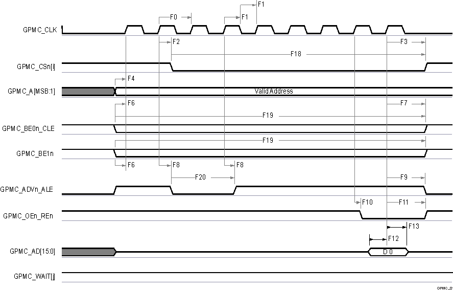
Table 7-63 and Table 7-64 present timing requirements and switching characteristics for GPMC and NOR Flash - Synchronous Mode.
Table 7-63 GPMC and NOR Flash Timing Requirements — Synchronous Mode see Figure 7-46,
Figure 7-47, and
Figure 7-50
| NO. | PARAMETER | DESCRIPTION | MODE(4) | MIN | MAX | MIN | MAX | UNIT |
|---|---|---|---|---|---|---|---|---|
| GPMC_FCLK = 100 MHz(1) | GPMC_FCLK = 133 MHz(1) | |||||||
| F12 | tsu(dV-clkH) | Setup time, input data GPMC_AD[15:0] valid before output clock GPMC_CLK high | div_by_1_mode; GPMC_FCLK_MUX; TIMEPARAGRANULARITY_X1 |
1.61 | 0.92 | ns | ||
| not_div_by_1_mode; GPMC_FCLK_MUX; TIMEPARAGRANULARITY_X1 |
0.86 | 3.41 | ns | |||||
| F13 | th(clkH-dV) | Hold time, input data GPMC_AD[15:0] valid after output clock GPMC_CLK high | div_by_1_mode; GPMC_FCLK_MUX; TIMEPARAGRANULARITY_X1 |
2.09 | 2.09 | ns | ||
| not_div_by_1_mode; GPMC_FCLK_MUX; TIMEPARAGRANULARITY_X1 |
2.09 | 2.09 | ns | |||||
| F21 | tsu(waitV-clkH) | Setup time, input wait GPMC_WAIT[j](2)(3) valid before output clock GPMC_CLK high | div_by_1_mode; GPMC_FCLK_MUX; TIMEPARAGRANULARITY_X1 |
1.61 | 0.92 | ns | ||
| not_div_by_1_mode; GPMC_FCLK_MUX; TIMEPARAGRANULARITY_X1 |
0.86 | 3.41 | ns | |||||
| F22 | th(clkH-waitV) | Hold time, input wait GPMC_WAIT[j](2)(3) valid after output clock GPMC_CLK high | div_by_1_mode; GPMC_FCLK_MUX; TIMEPARAGRANULARITY_X1 |
2.09 | 2.09 | ns | ||
| not_div_by_1_mode; GPMC_FCLK_MUX; TIMEPARAGRANULARITY_X1 |
2.09 | 2.09 | ns | |||||
(1) GPMC_FCLK select
- gpmc_fclk_sel[1:0] = 2b01 to select the 100MHz GPMC_FCLK
- gpmc_fclk_sel[1:0] = 2b00 to select the 133MHz GPMC_FCLK
(2) In
GPMC_WAIT[j], j is equal to 0 or 1.
(3) Wait
monitoring support is limited to a WaitMonitoringTime value > 0. For a full
description of wait monitoring feature, see General-Purpose Memory Controller
(GPMC) section in the device TRM.
(4) For
div_by_1_mode:
For not_div_by_1_mode:
For GPMC_FCLK_MUX:
For TIMEPARAGRANULARITY_X1:
- GPMC_CONFIG1_i Register:
GPMCFCLKDIVIDER = 0h:
- GPMC_CLK frequency = GPMC_FCLK frequency
For not_div_by_1_mode:
- GPMC_CONFIG1_i Register:
GPMCFCLKDIVIDER = 1h to 3h:
- GPMC_CLK frequency = GPMC_FCLK frequency / (2 to 4)
For GPMC_FCLK_MUX:
- CTRLMMR_GPMC_CLKSEL[1-0] CLK_SEL = 01 = PER1_PLL_CLKOUT / 3 = 300 / 3 = 100MHz
For TIMEPARAGRANULARITY_X1:
- GPMC_CONFIG1_i Register: TIMEPARAGRANULARITY = 0h = x1 latencies (affecting RD/WRCYCLETIME, RD/WRACCESSTIME, PAGEBURSTACCESSTIME, CSONTIME, CSRD/WROFFTIME, ADVONTIME, ADVRD/WROFFTIME, OEONTIME, OEOFFTIME, WEONTIME, WEOFFTIME, CYCLE2CYCLEDELAY, BUSTURNAROUND, TIMEOUTSTARTVALUE, WRDATAONADMUXBUS)
Table 7-64 GPMC and NOR Flash Switching Characteristics – Synchronous Mode see Figure 7-46,
Figure 7-47, Figure 7-48, Figure 7-49, and Figure 7-50
| NO.(2) | PARAMETER | DESCRIPTION | MODE(16) | MIN | MAX | MIN | MAX | UNIT |
|---|---|---|---|---|---|---|---|---|
| 100 MHz | 133 MHz | |||||||
| F0 | 1 / tc(clk) | Period, output clock GPMC_CLK(15) | div_by_1_mode; GPMC_FCLK_MUX; TIMEPARAGRANULARITY_X1 |
10.00 | 7.52 | ns | ||
| F1 | tw(clkH) | Typical pulse duration, output clock GPMC_CLK high | div_by_1_mode; GPMC_FCLK_MUX; TIMEPARAGRANULARITY_X1 |
0.475P - 0.3(14) | 0.475P - 0.3(14) | ns | ||
| F1 | tw(clkL) | Typical pulse duration, output clock GPMC_CLK low | div_by_1_mode; GPMC_FCLK_MUX; TIMEPARAGRANULARITY_X1 |
0.475P - 0.3(14) | 0.475P - 0.3(14) | ns | ||
| F2 | td(clkH-csnV) | Delay time, output clock GPMC_CLK rising edge to output chip select GPMC_CSn[i] transition(13) | div_by_1_mode; GPMC_FCLK_MUX; TIMEPARAGRANULARITY_X1; no extra_delay |
F - 2.2 (5) | F + 3.75 | F - 2.2 (5) | F + 3.75 | ns |
| F3 | td(clkH-CSn[i]V) | Delay time, output clock GPMC_CLK rising edge to output chip select GPMC_CSn[i] invalid(13) | div_by_1_mode; GPMC_FCLK_MUX; TIMEPARAGRANULARITY_X1; no extra_delay |
E - 2.2 (4) | E + 3.18 | E - 2.2 (4) | E + 4.5 | ns |
| F4 | td(aV-clk) | Delay time, output address GPMC_A[27:1] valid to output clock GPMC_CLK first edge | div_by_1_mode; GPMC_FCLK_MUX; TIMEPARAGRANULARITY_X1 |
B - 2.3 (2) | B + 4.5 | B - 2.3 (2) | B + 4.5 | ns |
| F5 | td(clkH-aIV) | Delay time, output clock GPMC_CLK rising edge to output address GPMC_A[27:1] invalid | div_by_1_mode; GPMC_FCLK_MUX; TIMEPARAGRANULARITY_X1 |
-2.3 | 4.5 | -2.3 | 4.5 | ns |
| F6 | td(be[x]nV-clk) | Delay time, output lower byte enable and command latch enable GPMC_BE0n_CLE, output upper byte enable GPMC_BE1n valid to output clock GPMC_CLK first edge | div_by_1_mode; GPMC_FCLK_MUX; TIMEPARAGRANULARITY_X1 |
B - 2.3 (2) | B + 1.9 | B - 2.3 (2) | B + 1.9 | ns |
| F7 | td(clkH-be[x]nIV) | Delay time, output clock GPMC_CLK rising edge to output lower byte enable and command latch enable GPMC_BE0n_CLE, output upper byte enable GPMC_BE1n invalid(10) | div_by_1_mode; GPMC_FCLK_MUX; TIMEPARAGRANULARITY_X1 |
D - 2.3(3) | D + 1.9 | D - 2.3 (3) | D + 1.9 | ns |
| F7 | td(clkL-be[x]nIV) | Delay time, GPMC_CLK falling edge to GPMC_BE0n_CLE, GPMC_BE1n invalid(11) | div_by_1_mode; GPMC_FCLK_MUX; TIMEPARAGRANULARITY_X1 |
D - 2.3 (3) | D + 1.9 | D - 2.3 (3) | D + 1.9 | ns |
| F7 | td(clkL-be[x]nIV). | Delay time, GPMC_CLK falling edge to GPMC_BE0n_CLE, GPMC_BE1n invalid(12) | div_by_1_mode; GPMC_FCLK_MUX; TIMEPARAGRANULARITY_X1 |
D - 2.3 (3) | D + 1.9 | D - 2.3 (3) | D + 1.9 | ns |
| F8 | td(clkH-advn) | Delay time, output clock GPMC_CLK rising edge to output address valid and address latch enable GPMC_ADVn_ALE transition | div_by_1_mode; GPMC_FCLK_MUX; TIMEPARAGRANULARITY_X1; no extra_delay |
G - 2.3(6) | G + 4.5 | G - 2.3 (6) | G + 4.5 | ns |
| F9 | td(clkH-advnIV) | Delay time, output clock GPMC_CLK rising edge to output address valid and address latch enable GPMC_ADVn_ALE invalid | div_by_1_mode; GPMC_FCLK_MUX; TIMEPARAGRANULARITY_X1; no extra_delay |
D - 2.3 (3) | D + 4.5 | D - 2.3 (3) | D + 4.5 | ns |
| F10 | td(clkH-oen) | Delay time, output clock GPMC_CLK rising edge to output enable GPMC_OEn_REn transition | div_by_1_mode; GPMC_FCLK_MUX; TIMEPARAGRANULARITY_X1; no extra_delay |
H - 2.3 (7) | H + 3.5 | H - 2.3 (7) | H + 3.5 | ns |
| F11 | td(clkH-oenIV) | Delay time, output clock GPMC_CLK rising edge to output enable GPMC_OEn_REn invalid | div_by_1_mode; GPMC_FCLK_MUX; TIMEPARAGRANULARITY_X1; no extra_delay |
H - 2.3 (7) | H + 3.5 | H - 2.3 (7) | H + 3.5 | ns |
| F14 | td(clkH-wen) | Delay time, output clock GPMC_CLK rising edge to output write enable GPMC_WEn transition | div_by_1_mode; GPMC_FCLK_MUX; TIMEPARAGRANULARITY_X1; no extra_delay |
I - 2.3 (8) | I + 4.5 | I - 2.3 (8) | I + 4.5 | ns |
| F15 | td(clkH-do) | Delay time, output clock GPMC_CLK rising edge to output data GPMC_AD[15:0] transition(10) | div_by_1_mode; GPMC_FCLK_MUX; TIMEPARAGRANULARITY_X1 |
J - 2.3 (9) | J + 2.7 | J - 2.3 (9) | J + 2.7 | ns |
| F15 | td(clkL-do) | Delay time, GPMC_CLK falling edge to GPMC_AD[15:0] data bus transition(11) | div_by_1_mode; GPMC_FCLK_MUX; TIMEPARAGRANULARITY_X1 |
J - 2.3 (9) | J + 2.7 | J - 2.3 (9) | J + 2.7 | ns |
| F15 | td(clkL-do). | Delay time, GPMC_CLK falling edge to GPMC_AD[15:0] data bus transition(12) | div_by_1_mode; GPMC_FCLK_MUX; TIMEPARAGRANULARITY_X1 |
J - 2.3 (9) | J + 2.7 | J - 2.3 (9) | J + 2.7 | ns |
| F17 | td(clkH-be[x]n) | Delay time, output clock GPMC_CLK rising edge to output lower byte enable and command latch enable GPMC_BE0n_CLE transition(10) | div_by_1_mode; GPMC_FCLK_MUX; TIMEPARAGRANULARITY_X1 |
J - 2.3 (9) | J + 1.9 | J - 2.3 (9) | J + 1.9 | ns |
| F17 | td(clkL-be[x]n) | Delay time, GPMC_CLK falling edge to GPMC_BE0n_CLE, GPMC_BE1n transition(11) | div_by_1_mode; GPMC_FCLK_MUX; TIMEPARAGRANULARITY_X1 |
J - 2.3 (9) | J + 1.9 | J - 2.3 (9) | J + 1.9 | ns |
| F17 | td(clkL-be[x]n). | Delay time, GPMC_CLK falling edge to GPMC_BE0n_CLE, GPMC_BE1n transition(12) | div_by_1_mode; GPMC_FCLK_MUX; TIMEPARAGRANULARITY_X1 |
J - 2.3 (9) | J + 1.9 | J - 2.3 (9) | J + 1.9 | ns |
| F18 | tw(csnV) | Pulse duration, output chip select GPMC_CSn[i](13) low | Read | A | A | ns | ||
| Write | A | A | ns | |||||
| F19 | tw(be[x]nV) | Pulse duration, output lower byte enable and command latch enable GPMC_BE0n_CLE, output upper byte enable GPMC_BE1n low | Read | C | C | ns | ||
| Write | C | C | ns | |||||
| F20 | tw(advnV) | Pulse duration, output address valid and address latch enable GPMC_ADVn_ALE low | Read | K | K | ns | ||
| Write | K | K | ns | |||||
(2) B =
ClkActivationTime × GPMC_FCLK(14)
(3) For
single read: D = (RdCycleTime - AccessTime) × (TimeParaGranularity + 1) ×
GPMC_FCLK(14)
For burst read: D = (RdCycleTime - AccessTime) × (TimeParaGranularity + 1) × GPMC_FCLK(14)
For burst write: D = (WrCycleTime - AccessTime) × (TimeParaGranularity + 1) × GPMC_FCLK(14)
For burst read: D = (RdCycleTime - AccessTime) × (TimeParaGranularity + 1) × GPMC_FCLK(14)
For burst write: D = (WrCycleTime - AccessTime) × (TimeParaGranularity + 1) × GPMC_FCLK(14)
(4) For
single read: E = (CSRdOffTime - AccessTime) × (TimeParaGranularity + 1) ×
GPMC_FCLK(14)
For burst read: E = (CSRdOffTime - AccessTime) × (TimeParaGranularity + 1) × GPMC_FCLK(14)
For burst write: E = (CSWrOffTime - AccessTime) × (TimeParaGranularity + 1) × GPMC_FCLK(14)
For burst read: E = (CSRdOffTime - AccessTime) × (TimeParaGranularity + 1) × GPMC_FCLK(14)
For burst write: E = (CSWrOffTime - AccessTime) × (TimeParaGranularity + 1) × GPMC_FCLK(14)
(5) For
csn falling edge (CS activated):
- Case GPMCFCLKDIVIDER = 0:
- F = 0.5 × CSExtraDelay × GPMC_FCLK(14)
- Case GPMCFCLKDIVIDER = 1:
- Case GPMCFCLKDIVIDER = 2:
- F = 0.5 × CSExtraDelay × GPMC_FCLK(14) if ((CSOnTime - ClkActivationTime) is a multiple of 3)
- F = (1 + 0.5 × CSExtraDelay) × GPMC_FCLK(14) if ((CSOnTime - ClkActivationTime - 1) is a multiple of 3)
- F = (2 + 0.5 × CSExtraDelay) × GPMC_FCLK(14) if ((CSOnTime - ClkActivationTime - 2) is a multiple of 3)
(6) For
ADV falling edge (ADV activated):
For ADV rising edge (ADV deactivated) in Reading mode:
For ADV rising edge (ADV deactivated) in Writing mode:
- Case GPMCFCLKDIVIDER = 0:
- G = 0.5 × ADVExtraDelay × GPMC_FCLK(14)
- Case GPMCFCLKDIVIDER = 1:
- Case GPMCFCLKDIVIDER = 2:
- G = 0.5 × ADVExtraDelay × GPMC_FCLK(14) if ((ADVOnTime - ClkActivationTime) is a multiple of 3)
- G = (1 + 0.5 × ADVExtraDelay) × GPMC_FCLK(14) if ((ADVOnTime - ClkActivationTime - 1) is a multiple of 3)
- G = (2 + 0.5 × ADVExtraDelay) × GPMC_FCLK(14) if ((ADVOnTime - ClkActivationTime - 2) is a multiple of 3)
For ADV rising edge (ADV deactivated) in Reading mode:
- Case GPMCFCLKDIVIDER = 0:
- G = 0.5 × ADVExtraDelay × GPMC_FCLK(14)
- Case GPMCFCLKDIVIDER = 1:
- Case GPMCFCLKDIVIDER = 2:
- G = 0.5 × ADVExtraDelay × GPMC_FCLK(14) if ((ADVRdOffTime - ClkActivationTime) is a multiple of 3)
- G = (1 + 0.5 × ADVExtraDelay) × GPMC_FCLK(14) if ((ADVRdOffTime - ClkActivationTime - 1) is a multiple of 3)
- G = (2 + 0.5 × ADVExtraDelay) × GPMC_FCLK(14) if ((ADVRdOffTime - ClkActivationTime - 2) is a multiple of 3)
For ADV rising edge (ADV deactivated) in Writing mode:
- Case GPMCFCLKDIVIDER = 0:
- G = 0.5 × ADVExtraDelay × GPMC_FCLK(14)
- Case GPMCFCLKDIVIDER = 1:
- Case GPMCFCLKDIVIDER = 2:
- G = 0.5 × ADVExtraDelay × GPMC_FCLK(14) if ((ADVWrOffTime - ClkActivationTime) is a multiple of 3)
- G = (1 + 0.5 × ADVExtraDelay) × GPMC_FCLK(14) if ((ADVWrOffTime - ClkActivationTime - 1) is a multiple of 3)
- G = (2 + 0.5 × ADVExtraDelay) × GPMC_FCLK(14) if ((ADVWrOffTime - ClkActivationTime - 2) is a multiple of 3)
(7) For
OE falling edge (OE activated) and IO DIR rising edge (Data Bus input
direction):
For OE rising edge (OE deactivated):
- Case GPMCFCLKDIVIDER = 0:
- H = 0.5 × OEExtraDelay × GPMC_FCLK(14)
- Case GPMCFCLKDIVIDER = 1:
- Case GPMCFCLKDIVIDER = 2:
- H = 0.5 × OEExtraDelay × GPMC_FCLK(14) if ((OEOnTime - ClkActivationTime) is a multiple of 3)
- H = (1 + 0.5 × OEExtraDelay) × GPMC_FCLK(14) if ((OEOnTime - ClkActivationTime - 1) is a multiple of 3)
- H = (2 + 0.5 × OEExtraDelay) × GPMC_FCLK(14) if ((OEOnTime - ClkActivationTime - 2) is a multiple of 3)
For OE rising edge (OE deactivated):
- Case GPMCFCLKDIVIDER = 0:
- H = 0.5 × OEExtraDelay × GPMC_FCLK(14)
- Case GPMCFCLKDIVIDER = 1:
- Case GPMCFCLKDIVIDER = 2:
- H = 0.5 × OEExtraDelay × GPMC_FCLK(14) if ((OEOffTime - ClkActivationTime) is a multiple of 3)
- H = (1 + 0.5 × OEExtraDelay) × GPMC_FCLK(14) if ((OEOffTime - ClkActivationTime - 1) is a multiple of 3)
- H = (2 + 0.5 × OEExtraDelay) × GPMC_FCLK(14) if ((OEOffTime - ClkActivationTime - 2) is a multiple of 3)
(8) For
WE falling edge (WE activated):
For WE rising edge (WE deactivated):
- Case GPMCFCLKDIVIDER = 0:
- I = 0.5 × WEExtraDelay × GPMC_FCLK(14)
- Case GPMCFCLKDIVIDER = 1:
- Case GPMCFCLKDIVIDER = 2:
- I = 0.5 × WEExtraDelay × GPMC_FCLK(14) if ((WEOnTime - ClkActivationTime) is a multiple of 3)
- I = (1 + 0.5 × WEExtraDelay) × GPMC_FCLK(14) if ((WEOnTime - ClkActivationTime - 1) is a multiple of 3)
- I = (2 + 0.5 × WEExtraDelay) × GPMC_FCLK(14) if ((WEOnTime - ClkActivationTime - 2) is a multiple of 3)
For WE rising edge (WE deactivated):
- Case GPMCFCLKDIVIDER = 0:
- I = 0.5 × WEExtraDelay × GPMC_FCLK (14)
- Case GPMCFCLKDIVIDER = 1:
- Case GPMCFCLKDIVIDER = 2:
- I = 0.5 × WEExtraDelay × GPMC_FCLK(14) if ((WEOffTime - ClkActivationTime) is a multiple of 3)
- I = (1 + 0.5 × WEExtraDelay) × GPMC_FCLK(14) if ((WEOffTime - ClkActivationTime - 1) is a multiple of 3)
- I = (2 + 0.5 × WEExtraDelay) × GPMC_FCLK(14) if ((WEOffTime - ClkActivationTime - 2) is a multiple of 3)
(9) J
= GPMC_FCLK(14)
(10) First transfer only for CLK DIV 1 mode.
(11) Half cycle; for all data after initial transfer for CLK DIV 1 mode.
(12) Half cycle of GPMC_CLKOUT; for all data for modes other than CLK DIV 1 mode.
GPMC_CLKOUT divide down from GPMC_FCLK.
(13) In
GPMC_CSn[i], i is equal to 0, 1, 2 or 3. In GPMC_WAIT[j], j is equal to 0 or
1.
(14) P
= GPMC_CLK period in ns
(15) Related to the GPMC_CLK output clock maximum and minimum frequencies
programmable in the GPMC module by setting the GPMC_CONFIG1_i configuration
register bit field GPMCFCLKDIVIDER.
(16) For div_by_1_mode:
For GPMC_FCLK_MUX:
For TIMEPARAGRANULARITY_X1:
For no extra_delay:
- GPMC_CONFIG1_i register:
GPMCFCLKDIVIDER = 0h:
- GPMC_CLK frequency = GPMC_FCLK frequency
For GPMC_FCLK_MUX:
- CTRLMMR_GPMC_CLKSEL[1-0] CLK_SEL = 01 = PER1_PLL_CLKOUT / 3 = 300 / 3 = 100MHz
For TIMEPARAGRANULARITY_X1:
- GPMC_CONFIG1_i Register: TIMEPARAGRANULARITY = 0h = x1 latencies (affecting RD/WRCYCLETIME, RD/WRACCESSTIME, PAGEBURSTACCESSTIME, CSONTIME, CSRD/WROFFTIME, ADVONTIME, ADVRD/WROFFTIME, OEONTIME, OEOFFTIME, WEONTIME, WEOFFTIME, CYCLE2CYCLEDELAY, BUSTURNAROUND, TIMEOUTSTARTVALUE, WRDATAONADMUXBUS)
For no extra_delay:
- GPMC_CONFIG2_i Register: CSEXTRADELAY = 0h = CSn Timing control signal is not delayed
- GPMC_CONFIG4_i Register: WEEXTRADELAY = 0h = nWE timing control signal is not delayed
- GPMC_CONFIG4_i Register: OEEXTRADELAY = 0h = nOE timing control signal is not delayed
- GPMC_CONFIG3_i Register: ADVEXTRADELAY = 0h = nADV timing control signal is not delayed
A. In GPMC_CSn[i], i is equal to 0,
1, 2 or 3.
B. In GPMC_WAIT[j], j is equal to 0
or 1.
Figure 7-46 GPMC and
NOR Flash — Synchronous Single Read (GPMCFCLKDIVIDER = 0) 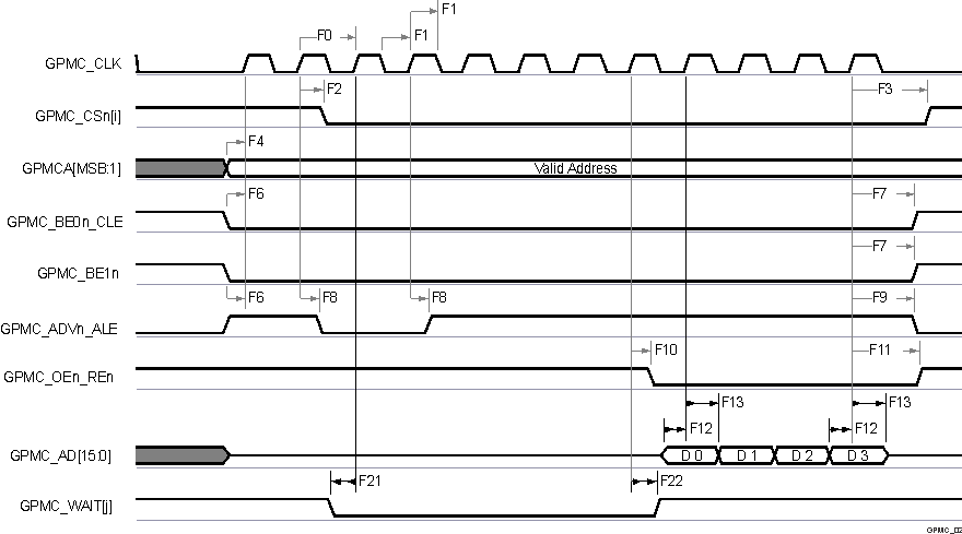
A. In GPMC_CSn[i], i is equal to 0,
1, 2 or 3.
B. In GPMC_WAIT[j], j is equal to 0
or 1.
Figure 7-47 GPMC and
NOR Flash — Synchronous Burst Read — 4x16–bit (GPMCFCLKDIVIDER = 0) 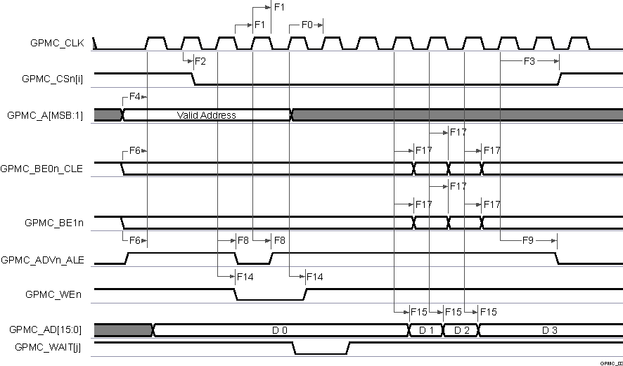
A. In GPMC_CSn[i], i is equal to 0,
1, 2 or 3.
B. In GPMC_WAIT[j], j is equal to 0
or 1.
Figure 7-48 GPMC and
NOR Flash—Synchronous Burst Write (GPMCFCLKDIVIDER = 0) 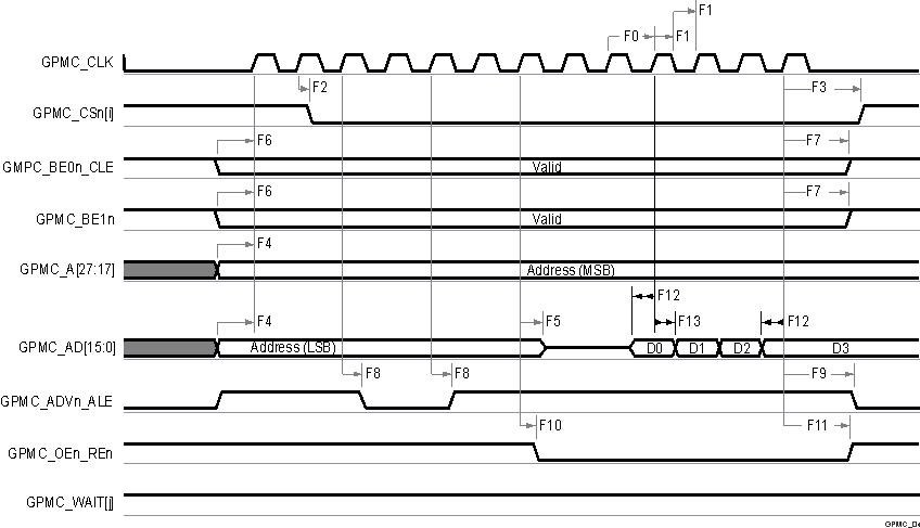
A. In GPMC_CSn[i], i is equal to 0,
1, 2 or 3.
B. In GPMC_WAIT[j], j is equal to 0
or 1.
Figure 7-49 GPMC and
Multiplexed NOR Flash — Synchronous Burst Read 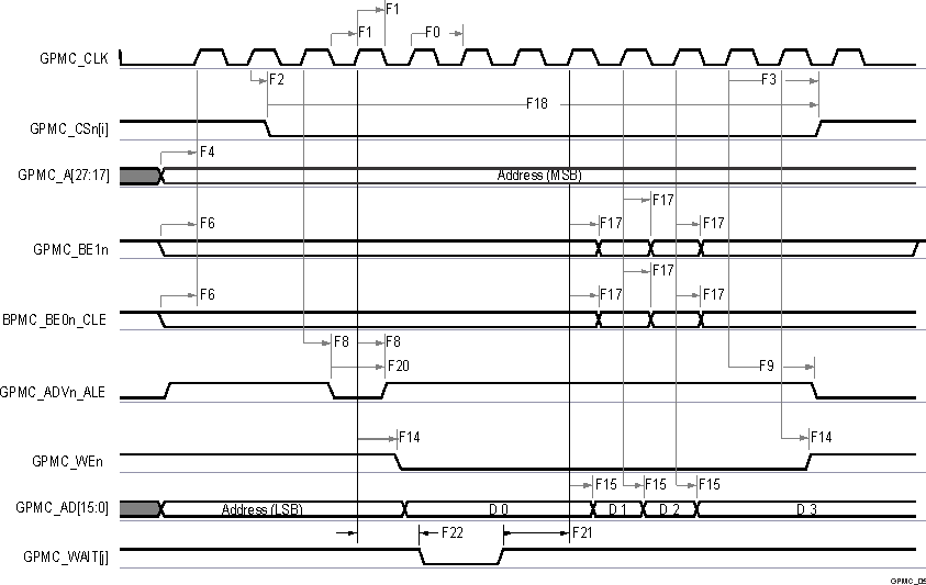
A. In GPMC_CSn[i], i is equal to 0,
1, 2 or 3.
B. In GPMC_WAIT[j], j is equal to 0
or 1.
Figure 7-50 GPMC and
Multiplexed NOR Flash — Synchronous Burst Write