SPRSP58B june 2022 – june 2023 AM620-Q1 , AM623 , AM625 , AM625-Q1
PRODUCTION DATA
- 1
- 1 Features
- 2 Applications
- 3 Description
- 4 Revision History
- 5 Device Comparison
-
6 Terminal Configuration and Functions
- 6.1 Pin Diagrams
- 6.2 Pin Attributes
- 6.3
Signal Descriptions
- 15
- 6.3.1 CPSW3G
- 6.3.2 CPTS
- 6.3.3 CSI-2
- 6.3.4 DDRSS
- 6.3.5 DSS
- 6.3.6 ECAP
- 6.3.7 Emulation and Debug
- 6.3.8 EPWM
- 6.3.9 EQEP
- 6.3.10 GPIO
- 6.3.11 GPMC
- 6.3.12 I2C
- 6.3.13 MCAN
- 6.3.14 MCASP
- 6.3.15 MCSPI
- 6.3.16 MDIO
- 6.3.17 MMC
- 6.3.18 OLDI
- 6.3.19 OSPI
- 6.3.20 Power Supply
- 6.3.21 PRUSS
- 6.3.22 Reserved
- 6.3.23 System and Miscellaneous
- 6.3.24 TIMER
- 6.3.25 UART
- 6.3.26 USB
- 6.4 Pin Connectivity Requirements
-
7 Specifications
- 7.1 Absolute Maximum Ratings
- 7.2 ESD Ratings for Devices which are not AEC - Q100 Qualified
- 7.3 ESD Ratings for AEC - Q100 Qualified Devices in the AMC Package
- 7.4 Power-On Hours (POH)
- 7.5 Recommended Operating Conditions
- 7.6 Operating Performance Points
- 7.7 Power Consumption Summary
- 7.8
Electrical
Characteristics
- 7.8.1 I2C Open-Drain, and Fail-Safe (I2C OD FS) Electrical Characteristics
- 7.8.2 Fail-Safe Reset (FS RESET) Electrical Characteristics
- 7.8.3 High-Frequency Oscillator (HFOSC) Electrical Characteristics
- 7.8.4 Low-Frequency Oscillator (LFXOSC) Electrical Characteristics
- 7.8.5 SDIO Electrical Characteristics
- 7.8.6 LVCMOS Electrical Characteristics
- 7.8.7 OLDI LVDS (OLDI) Electrical Characteristics
- 7.8.8 CSI-2 (D-PHY) Electrical Characteristics
- 7.8.9 USB2PHY Electrical Characteristics
- 7.8.10 DDR Electrical Characteristics
- 7.9 VPP Specifications for One-Time Programmable (OTP) eFuses
- 7.10 Thermal Resistance Characteristics
- 7.11
Timing and Switching Characteristics
- 7.11.1 Timing Parameters and Information
- 7.11.2 Power Supply Requirements
- 7.11.3 System Timing
- 7.11.4
Clock Specifications
- 7.11.4.1 Input Clocks / Oscillators
- 7.11.4.2 Output Clocks
- 7.11.4.3 PLLs
- 7.11.4.4 Recommended System Precautions for Clock and Control Signal Transitions
- 7.11.5
Peripherals
- 7.11.5.1 CPSW3G
- 7.11.5.2 CPTS
- 7.11.5.3 CSI-2
- 7.11.5.4 DDRSS
- 7.11.5.5 DSS
- 7.11.5.6 ECAP
- 7.11.5.7 Emulation and Debug
- 7.11.5.8 EPWM
- 7.11.5.9 EQEP
- 7.11.5.10 GPIO
- 7.11.5.11 GPMC
- 7.11.5.12 I2C
- 7.11.5.13 MCAN
- 7.11.5.14 MCASP
- 7.11.5.15 MCSPI
- 7.11.5.16
MMCSD
- 7.11.5.16.1
MMC0 - eMMC/SD/SDIO Interface
- 7.11.5.16.1.1 Legacy SDR Mode
- 7.11.5.16.1.2 High Speed SDR Mode
- 7.11.5.16.1.3 HS200 Mode
- 7.11.5.16.1.4 Default Speed Mode
- 7.11.5.16.1.5 High Speed Mode
- 7.11.5.16.1.6 UHS–I SDR12 Mode
- 7.11.5.16.1.7 UHS–I SDR25 Mode
- 7.11.5.16.1.8 UHS–I SDR50 Mode
- 7.11.5.16.1.9 UHS–I DDR50 Mode
- 7.11.5.16.1.10 UHS–I SDR104 Mode
- 7.11.5.16.2 MMC1/MMC2 - SD/SDIO Interface
- 7.11.5.16.1
MMC0 - eMMC/SD/SDIO Interface
- 7.11.5.17 OLDI
- 7.11.5.18 OSPI
- 7.11.5.19 PRUSS
- 7.11.5.20 Timers
- 7.11.5.21 UART
- 7.11.5.22 USB
-
8 Detailed Description
- 8.1 Overview
- 8.2 Processor Subsystems
- 8.3 Accelerators and Coprocessors
- 8.4 Other Subsystems
- 8.5
Peripherals
- 8.5.1 Gigabit Ethernet Switch (CPSW3G)
- 8.5.2 Camera Streaming Interface Receiver (CSI_RX_IF)
- 8.5.3 DDR Subsystem (DDRSS)
- 8.5.4 Display Subsystem (DSS)
- 8.5.5 Enhanced Capture (ECAP)
- 8.5.6 Error Location Module (ELM)
- 8.5.7 Enhanced Pulse Width Modulation (EPWM)
- 8.5.8 Error Signaling Module (ESM)
- 8.5.9 Enhanced Quadrature Encoder Pulse (EQEP)
- 8.5.10 General-Purpose Interface (GPIO)
- 8.5.11 General-Purpose Memory Controller (GPMC)
- 8.5.12 Global Timebase Counter (GTC)
- 8.5.13 Inter-Integrated Circuit (I2C)
- 8.5.14 Modular Controller Area Network (MCAN)
- 8.5.15 Multichannel Audio Serial Port (MCASP)
- 8.5.16 Multichannel Serial Peripheral Interface (MCSPI)
- 8.5.17 Multi-Media Card Secure Digital (MMCSD)
- 8.5.18 Octal Serial Peripheral Interface (OSPI)
- 8.5.19 Timers
- 8.5.20 Universal Asynchronous Receiver/Transmitter (UART)
- 8.5.21 Universal Serial Bus Subsystem (USBSS)
-
9 Applications,
Implementation, and Layout
- 9.1 Device Connection and Layout Fundamentals
- 9.2 Peripheral- and Interface-Specific Design Information
- 10Device and Documentation Support
- 11Mechanical, Packaging, and Orderable Information
Package Options
Refer to the PDF data sheet for device specific package drawings
Mechanical Data (Package|Pins)
- ALW|425
Thermal pad, mechanical data (Package|Pins)
Orderable Information
7.11.4.1.1.2 Shunt Capacitance
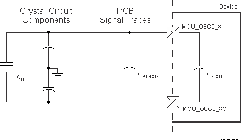
The crystal circuit must also be designed such that it does not exceed the maximum shunt capacitance for MCU_OSC0 operating conditions defined in Table 7-21. Shunt capacitance, Cshunt, of the crystal circuit is a combination of crystal shunt capacitance and parasitic contributions. PCB signal traces which connect crystal circuit components to MCU_OSC0 have mutual parasitic capacitance to each other, CPCBXIXO, where the PCB designer should be able to extract mutual parasitic capacitance between these signal traces. The device package also has mutual parasitic capacitance, CXIXO, where this mutual parasitic capacitance value is defined in Table 7-22.
PCB routing should be designed to minimize mutual capacitance between XI and XO signal traces. This is typically done by keeping signal traces short and not routing them in close proximity. Mutual capacitance can also be minimized by placing a ground trace between these signals when the layout requires them to be routed in close proximity. It is important to minimize the mutual capacitance on the PCB to provide as much margin as possible when selecting a crystal.
 Figure 7-19 Shunt Capacitance
A crystal should be chosen such that the below equation is satisfied. CO in the equation is the maximum shunt capacitance specified by the crystal manufacturer.
Cshunt ≥ CO + CPCBXIXO + CXIXO
For example, the equation would be satisfied when the crystal being used is 25 MHz with an ESR = 30 Ω, CPCBXIXO = 0.04 pF, CXIXO = 0.01 pF, and shunt capacitance of the crystal is less than or equal to 6.95 pF.