SBAS585A September   2012  – January 2016 AMC1200-Q1

PRODUCTION DATA.  

  1. Features
  2. Applications
  3. Description
  4. Revision History
  5. Pin Configurations and Functions
  6. Specifications
    1. 6.1 Absolute Maximum Ratings
    2. 6.2 ESD Ratings
    3. 6.3 Recommended Operating Conditions
    4. 6.4 Thermal Information
    5. 6.5 Electrical Characteristics
    6. 6.6 Typical Characteristics
  7. Detailed Description
    1. 7.1 Overview
    2. 7.2 Functional Block Diagram
    3. 7.3 Feature Description
      1. 7.3.1 Insulation Characteristics
      2. 7.3.2 IEC Safety Limiting Values
      3. 7.3.3 Package Characteristics
      4. 7.3.4 Regulatory Information
      5. 7.3.5 Analog Input
    4. 7.4 Device Functional Modes
  8. Application and Implementation
    1. 8.1 Application Information
    2. 8.2 Typical Applications
      1. 8.2.1 Traction Inverter
        1. 8.2.1.1 Design Requirements
        2. 8.2.1.2 Detailed Design Procedure
        3. 8.2.1.3 Application Curves
      2. 8.2.2 Isolated Voltage Measurement
  9. Power Supply Recommendations
  10. 10Layout
    1. 10.1 Layout Guidelines
    2. 10.2 Layout Example
  11. 11Device and Documentation Support
    1. 11.1 Documentation Support
      1. 11.1.1 Related Documentation
    2. 11.2 Community Resources
    3. 11.3 Trademarks
    4. 11.4 Electrostatic Discharge Caution
    5. 11.5 Glossary
  12. 12Mechanical, Packaging, and Orderable Information

Package Options

Mechanical Data (Package|Pins)
Thermal pad, mechanical data (Package|Pins)
Orderable Information

6 Specifications

6.1 Absolute Maximum Ratings

over operating ambient temperature range (unless otherwise noted)(1)
MIN MAX UNIT
Supply voltage VDD1 to GND1 or VDD2 to GND2 –0.5 6 V
Input voltage VINP, VINN GND1 – 0.5 VDD1 + 0.5 V
Input current VINP, VINN, VOUTP, VOUTN –10 10 mA
Junction temperature, TJ –40 150 °C
Storage temperature, Tstg –65 150 °C
(1) Stresses beyond those listed under Absolute Maximum Ratings may cause permanent damage to the device. These are stress ratings only, and functional operation of the device at these or any other conditions beyond those indicated is not implied. Exposure to absolute maximum rated conditions for extended periods may affect device reliability.

6.2 ESD Ratings

VALUE UNIT
V(ESD) Electrostatic discharge Human-body model (HBM), per AEC-Q100, Classification Level H2(1) ±2500 V
Charged-device model (CDM), per AEC-Q100, Classification Level C3B(2) ±1000
(1) JEDEC document JEP155 states that 500-V HBM allows safe manufacturing with a standard ESD control process.
(2) JEDEC document JEP157 states that 250-V CDM allows safe manufacturing with a standard ESD control process.

6.3 Recommended Operating Conditions

over operating ambient temperature range (unless otherwise noted)
MIN NOM MAX UNIT
VDD1 High-side supply voltage 4.5 5 5.5 V
VDD2 Low-side supply voltage 2.7 5 5.5 V
VVINP, VVINN Absolute input voltage GND1 – 0.32 VDD1 + 0.16 V
VIN Differential input voltage VVINP – VVINN –250 250 mV
VCM Common-mode input voltage (VVINP + VVIN) / 2 GND1 – 0.16 VDD1 V
TA Operating ambient temperature –40 25 105 °C

6.4 Thermal Information

THERMAL METRIC(1) AMC1200-Q1 UNIT
DUB (SOP) DWV (SOIC)
8 PINS 8 PINS
RθJA Junction-to-ambient thermal resistance 75.1 102.8 °C/W
RθJC(top) Junction-to-case (top) thermal resistance 61.6 49.8 °C/W
RθJB Junction-to-board thermal resistance 39.8 56.6 °C/W
ψJT Junction-to-top characterization parameter 27.2 16 °C/W
ψJB Junction-to-board characterization parameter 39.4 55.2 °C/W
(1) For more information about traditional and new thermal metrics, see the Semiconductor and IC Package Thermal Metrics application report, SPRA953.

6.5 Electrical Characteristics

Minimum and maximum specifications are at TA = –40°C to +105°C, VDD1 = 4.5 V to 5.5 V, and VDD2 = 2.7 V to 5.5 V. Typical specifications are at TA = 25°C, VDD1 = 5 V, and VDD2 = 3.3 V (unless otherwise noted).
PARAMETER TEST CONDITIONS MIN TYP MAX UNIT
INPUT
VClipping Input voltage with clipping output VVINP – VVINN ±320 mV
VIO Input offset voltage –1.5 ±0.2 1.5 mV
Input offset thermal drift –10 ±1.5 10 µV/°C
CMRR Common-mode rejection ratio VIN from 0 V to 5 V at 0 Hz 108 dB
VIN from 0 V to 5 V at 50 kHz 95
CI Input capacitance VINP to GND1 or VINN to GND1 3 pF
CID Differential input capacitance 3.6 pF
RID Differential input resistance 28
Small-signal bandwidth 60 100 kHz
OUTPUT
G Nominal gain 8
EG Gain error Initial, TA = 25°C –0.5% ±0.05% 0.5%
–1% ±0.05% 1%
Gain error thermal drift ±56 ppm/°C
Nonlinearity 4.5 V ≤ VDD2 ≤ 5.5 V –0.075% ±0.015% 0.075%
2.7 V ≤ VDD2 ≤ 3.6 V –0.1% ±0.023% 0.1%
Nonlinearity thermal drift 2.4 ppm/°C
Output noise VVINP = VVINN = 0 V 3.1 mVRMS
PSRR Power-supply rejection ratio PSRR vs VDD1, 10-kHz ripple 80 dB
PSRR vs VDD2, 10-kHz ripple 61
Rise and fall time 0.5-V step, 10% to 90% 3.66 6.6 µs
VIN to VOUT signal delay 0.5-V step, 50% to 10%, unfiltered output 1.6 3.3 µs
0.5-V step, 50% to 50%, unfiltered output 3.15 5.6
0.5-V step, 50% to 90%, unfiltered output 5.26 9.9
CMTI Common-mode transient immunity VCM = 1 kV, TA = 25°C 8 15 kV/µs
Output common-mode voltage 2.7 V ≤ VDD2 ≤ 3.6 V 1.15 1.29 1.45 V
4.5 V ≤ VDD2 ≤ 5.5 V 2.4 2.55 2.7
Short-circuit current 20 mA
RO Output resistance 2.5 Ω
POWER SUPPLY
IDD1 High-side supply current 5.4 8 mA
IDD2 Low-side supply current 2.7 V ≤ VDD2 ≤ 3.6 V 3.8 6 mA
4.5 V ≤ VDD2 ≤ 5.5 V 4.4 7
PDD1 High-side power dissipation 27 44 mW
PDD2 Low-side power dissipation 2.7 V≤ VDD2 ≤ 3.6 V 11.4 21.6 mW
4.5 V ≤ VDD2 ≤ 5.5 V 22 38.5

6.6 Typical Characteristics

TA = 25°C, VDD1 = VDD2 = 5 V, VVINP = –250 mV to 250 mV, and VVINN = 0 V (unless otherwise noted)
AMC1200-Q1 tc_offset-vdd1_bas542.png
Figure 1. Input Offset vs High-Side Supply Voltage
AMC1200-Q1 tc_offset-vdd2_45v_bas542.png
Figure 3. Input Offset vs Low-Side Supply Voltage
AMC1200-Q1 tc_cmrr-frq_bas542.png
Figure 5. Common-Mode Rejection Ratio
vs Input Frequency
AMC1200-Q1 tc_bw-tmp_bas542.png
Figure 7. Input Bandwidth vs Temperature
AMC1200-Q1 tc_gain-vdd2_27v_bas542.png
Figure 9. Gain Error vs Low-Side Supply Voltage
AMC1200-Q1 tc_gain-tmp_bas542.png
Figure 11. Gain Error vs Temperature
AMC1200-Q1 tc_phase-frq_bas542.png
Figure 13. Output Phase vs Input Frequency
AMC1200-Q1 tc_vout-vin_27v_bas542.png
Figure 15. Output Voltage vs Input Voltage
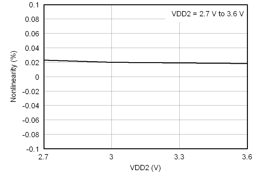
AMC1200-Q1 tc_nonlinearity-vdd2_27v_bas542.png
Figure 17. Nonlinearity vs Low-Side Supply Voltage
AMC1200-Q1 tc_nonlinearity-vin_bas542.png
Figure 19. Nonlinearity vs Input Voltage
AMC1200-Q1 tc_noise-frq_bas542.png
Figure 21. Output Noise Density vs Frequency
AMC1200-Q1 tc_rise_fall-tmp_bas542.png
Figure 23. Output Rise and Fall Time vs Temperature
AMC1200-Q1 tc_delay-tmp_bas542.png
Figure 25. Output Signal Delay Time vs Temperature
AMC1200-Q1 tc_vcm-tmp_bas542.png
Figure 27. Output Common-Mode Voltage vs Temperature
AMC1200-Q1 tc_ivdd2-vdd2_bas542.png
Figure 29. Low-Side Supply Current
vs Low-Side Supply Voltage
AMC1200-Q1 tc_offset-vdd2_27v_bas542.png
Figure 2. Input Offset vs Low-Side Supply Voltage
AMC1200-Q1 tc_offset-tmp_bas542.png
Figure 4. Input Offset vs Temperature
AMC1200-Q1 tc_iin-vin_bas542.png
Figure 6. Input Current vs Input Voltage
AMC1200-Q1 tc_gain-vdd1_bas542.png
Figure 8. Gain Error vs High-Side Supply Voltage
AMC1200-Q1 tc_gain-vdd2_45v_bas542.png
Figure 10. Gain Error vs Low-Side Supply Voltage
AMC1200-Q1 tc_gain-frq_bas542.png
Figure 12. Normalized Gain vs Input Frequency
AMC1200-Q1 tc_vout-vin_bas542.png
Figure 14. Output Voltage vs Input Voltage
AMC1200-Q1 tc_nonlinearity-vdd1_bas542.png
Figure 16. Nonlinearity vs High-Side Supply Voltage
AMC1200-Q1 tc_nonlinearity-vdd2_45v_bas542.png
Figure 18. Nonlinearity vs Low-Side Supply Voltage
AMC1200-Q1 tc_nonlinearity-tmp_bas542.png
Figure 20. Nonlinearity vs Temperature
AMC1200-Q1 tc_psrr-frq_bas542.png
Figure 22. Power-Supply Rejection Ratio
vs Ripple Frequency
AMC1200-Q1 tc_step_response_bas542.gif
Figure 24. Full-Scale Step Response
AMC1200-Q1 tc_vcm-vdd2_bas542.png
Figure 26. Output Common-Mode Voltage
vs Low-Side Supply Voltage
AMC1200-Q1 tc_idd-vdd_bas542.png
Figure 28. Supply Current vs Supply Voltage
AMC1200-Q1 tc_idd-tmp_bas542.png
Figure 30. Supply Current vs Temperature