SBASAC9B February 2022 – December 2024 AMC23C11
PRODUCTION DATA
- 1
- 1 Features
- 2 Applications
- 3 Description
- 4 Pin Configuration and Functions
-
5 Specifications
- 5.1 Absolute Maximum Ratings
- 5.2 ESD Ratings
- 5.3 Recommended Operating Conditions
- 5.4 Thermal Information
- 5.5 Power Ratings
- 5.6 Insulation Specifications (Reinforced Isolation)
- 5.7 Safety-Related Certifications
- 5.8 Safety Limiting Values
- 5.9 Electrical Characteristics
- 5.10 Switching Characteristics
- 5.11 Timing Diagrams
- 5.12 Insulation Characteristics Curves
- 5.13 Typical Characteristics
- 6 Detailed Description
- 7 Application and Implementation
- 8 Device and Documentation Support
- 9 Revision History
- 10Mechanical, Packaging, and Orderable Information
Package Options
Mechanical Data (Package|Pins)
- DWV|8
Thermal pad, mechanical data (Package|Pins)
Orderable Information
3 Description
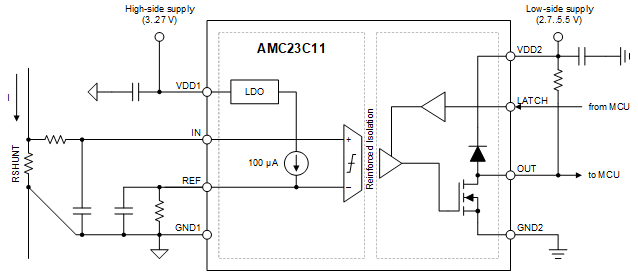
The AMC23C11 is an isolated comparator with a short response time. The open-drain output is separated from the input circuitry by an isolation barrier that is highly resistant to magnetic interference. This barrier is certified to provide reinforced galvanic isolation of up to 5kVRMS according to VDE 0884-17 and UL1577, and supports a working voltage of up to 1kVRMS.
The trip threshold is adjustable from 20mV to 450mV in low-hysteresis mode and from 600mV to 2.7V in high-hysteresis mode through a single external resistor.
The open-drain output on the device supports transparent mode (LATCH input tied to GND2) where the output follows the input state, or latch mode, where the output is cleared on the falling edge of the latch input signal.
The AMC23C11 is available in an 8-pin, wide-body SOIC package and is specified over the extended industrial temperature range of –40°C to +125°C.
 Typical Application