SWRS248D April 2020 – January 2022 AWR6443 , AWR6843
PRODUCTION DATA
- 1 Features
- 2 Applications
- 3 Description
- 4 Functional Block Diagram
- 5 Device Comparison
- 6 Terminal Configuration and Functions
-
7 Specifications
- 7.1 Absolute Maximum Ratings
- 7.2 ESD Ratings
- 7.3 Power-On Hours (POH)
- 7.4 Recommended Operating Conditions
- 7.5 Power Supply Specifications
- 7.6 Power Consumption Summary
- 7.7 RF Specification
- 7.8 CPU Specifications
- 7.9 Thermal Resistance Characteristics for FCBGA Package [ABL0161]
- 7.10
Timing and Switching Characteristics
- 7.10.1 Power Supply Sequencing and Reset Timing
- 7.10.2 Input Clocks and Oscillators
- 7.10.3 Multibuffered / Standard Serial Peripheral Interface (MibSPI)
- 7.10.4 LVDS Interface Configuration
- 7.10.5 General-Purpose Input/Output
- 7.10.6 Controller Area Network - Flexible Data-rate (CAN-FD)
- 7.10.7 Serial Communication Interface (SCI)
- 7.10.8 Inter-Integrated Circuit Interface (I2C)
- 7.10.9 Quad Serial Peripheral Interface (QSPI)
- 7.10.10 ETM Trace Interface
- 7.10.11 Data Modification Module (DMM)
- 7.10.12 JTAG Interface
- 8 Detailed Description
- 9 Monitoring and Diagnostics
- 10Applications, Implementation, and Layout
- 11Device and Documentation Support
- 12Mechanical, Packaging, and Orderable Information
Package Options
Refer to the PDF data sheet for device specific package drawings
Mechanical Data (Package|Pins)
- ABL|161
Thermal pad, mechanical data (Package|Pins)
Orderable Information
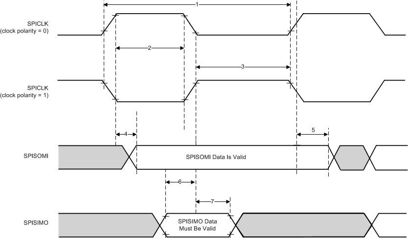
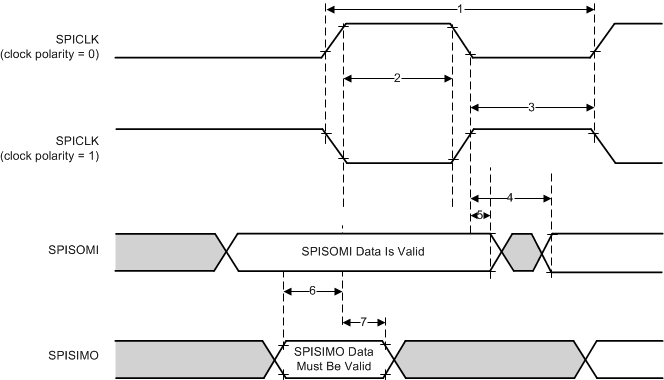
7.10.3.3.1 SPI Peripheral Mode Switching Parameters
(SPICLK = input, SPISIMO = input,
and SPISOMI =
output)(1)(2)(3)
| NO. | PARAMETER | MIN | TYP | MAX | UNIT | |
|---|---|---|---|---|---|---|
| 1 | tc(SPC)S | Cycle time, SPICLK(4) | 25 | ns | ||
| 2(5) | tw(SPCH)S | Pulse duration, SPICLK high (clock polarity = 0) | 10 | ns | ||
| tw(SPCL)S | Pulse duration, SPICLK low (clock polarity = 1) | 10 | ||||
| 3(5) | tw(SPCL)S | Pulse duration, SPICLK low (clock polarity = 0) | 10 | ns | ||
| tw(SPCH)S | Pulse duration, SPICLK high (clock polarity = 1) | 10 | ||||
| 4(5) | td(SPCH-SOMI)S | Delay time, SPISOMI valid after SPICLK high (clock polarity = 0) | 10 | ns | ||
| td(SPCL-SOMI)S | Delay time, SPISOMI valid after SPICLK low (clock polarity = 1) | 10 | ||||
| 5(5) | th(SPCH-SOMI)S | Hold time, SPISOMI data valid after SPICLK high (clock polarity = 0) | 2 | ns | ||
| th(SPCL-SOMI)S | Hold time, SPISOMI data valid after SPICLK low (clock polarity = 1) | 2 | ||||
| 4(5) | td(SPCH-SOMI)S | Delay time, SPISOMI valid after SPICLK high (clock polarity = 0; clock phase = 0) OR (clock polarity = 1; clock phase = 1) | 10 | ns | ||
| td(SPCL-SOMI)S | Delay time, SPISOMI valid after SPICLK low (clock polarity = 1; clock phase = 0) OR (clock polarity = 0; clock phase = 1) | 10 | ||||
| 5(5) | th(SPCH-SOMI)S | Hold time, SPISOMI data valid after SPICLK high (clock polarity = 0; clock phase = 0) OR (clock polarity = 1; clock phase = 1) | 2 | ns | ||
| th(SPCL-SOMI)S | Hold time, SPISOMI data valid after SPICLK low (clock polarity = 1; clock phase = 0) OR (clock polarity = 0; clock phase = 1) | 2 | ||||
| 6(5) | tsu(SIMO-SPCL)S | Setup time, SPISIMO before SPICLK low (clock polarity = 0; clock phase = 0) OR (clock polarity = 1; clock phase = 1) | 3 | ns | ||
| tsu(SIMO-SPCH)S | Setup time, SPISIMO before SPICLK high (clock polarity = 1; clock phase = 0) OR (clock polarity = 0; clock phase = 1) | 3 | ||||
| 7(5) | th(SPCL-SIMO)S | Hold time, SPISIMO data valid after SPICLK low (clock polarity = 0; clock phase = 0) OR (clock polarity = 1; clock phase = 1) | 1 | ns | ||
| th(SPCL-SIMO)S | Hold time, SPISIMO data valid after SPICLK high (clock polarity = 1; clock phase = 0) OR (clock polarity = 0; clock phase = 1) | 1 | ||||
(1) The MASTER bit (SPIGCRx.0) is cleared ( where x = 0 or 1 ).
(2) The CLOCK PHASE bit (SPIFMTx.16) is either cleared or set for CLOCK PHASE = 0 or CLOCK PHASE = 1 respectively.
(3) tc(MSS_VCLK) = main subsystem clock time = 1 /
f(MSS_VCLK). For more details, see the Technical Reference
Manual.
(4) When the SPI is in Peripheral mode, the following must be true: For PS values
from 1 to 255: tc(SPC)S ≥ (PS
+1)tc(MSS_VCLK) ≥ 25 ns, where PS is
the prescale value set in the SPIFMTx.[15:8]
register bits.For PS values of 0:
tc(SPC)S = 2tc(MSS_VCLK) ≥
25 ns.
(5) The active edge of the SPICLK signal referenced is controlled by the CLOCK POLARITY bit (SPIFMTx.17).
 Figure 7-8 SPI Peripheral Mode
External Timing (CLOCK PHASE = 0)
 Figure 7-9 SPI Peripheral Mode
External Timing (CLOCK PHASE = 1)