SLUS893B March 2010 – June 2015
PRODUCTION DATA.
- 1 Features
- 2 Applications
- 3 Description
- 4 Revision History
- 5 Device Comparison Table
- 6 Pin Configuration and Functions
- 7 Specifications
-
8 Detailed Description
- 8.1 Overview
- 8.2 Functional Block Diagram
- 8.3
Feature Description
- 8.3.1 Battery Voltage Regulation
- 8.3.2 Battery Current Regulation
- 8.3.3 Precharge
- 8.3.4 Charge Termination, Recharge, and Safety Timer
- 8.3.5 Power Up
- 8.3.6 Enable and Disable Charging
- 8.3.7 Automatic Internal Soft-Start Charger Current
- 8.3.8 Converter Operation
- 8.3.9 Synchronous and Nonsynchronous Operation
- 8.3.10 Cycle-by-Cycle Charge Undercurrent
- 8.3.11 Input Overvoltage Protection (ACOV)
- 8.3.12 Input Undervoltage Lockout (UVLO)
- 8.3.13 Battery Overvoltage Protection
- 8.3.14 Cycle-by-Cycle Charge Overcurrent Protection
- 8.3.15 Thermal Shutdown Protection
- 8.3.16 Temperature Qualification
- 8.3.17 Timer Fault Recovery
- 8.3.18 PG Output
- 8.3.19 CE (Charge Enable)
- 8.3.20 Charge Status Outputs
- 8.3.21 Battery Detection
- 8.4 Device Functional Modes
- 9 Application and Implementation
- 10Power Supply Recommendations
- 11Layout
- 12Device and Documentation Support
- 13Mechanical, Packaging, and Orderable Information
Package Options
Mechanical Data (Package|Pins)
- RVA|16
Thermal pad, mechanical data (Package|Pins)
- RVA|16
Orderable Information
8 Detailed Description
8.1 Overview
The bq24620 device is a stand-alone, integrated lithium phosphate battery charger. The device employs a switched-mode synchronous buck PWM controller with constant switching frequency.
The bq24620 has a battery detect scheme that allows it to automatically detect the presence and absence of a battery. When the battery is detected, charging begins in one of three phases (depending upon battery voltage): precharge, constant current (fast-charge current regulation), and constant voltage (fast-charge voltage regulation). The device will terminate charging when the termination current threshold has been reached and will begin a recharge cycle when the battery voltage has dropped below the recharge threshold (VRECHG). Constant (fastcharge) current and termination current can be configured through the ISET pin, allowing for flexibility in battery charging profile. During charging, the integrated fault monitors of the device, such as battery overvoltage protection, battery short detection (VBATSHT), thermal shutdown (internal TSHUT and TS pin), and input voltage protection (VACOV and VUVLO), ensure battery safety.
The bq24620 has two status pins (STAT and PG) to indicate the charging status and input voltage (AC adapter) status. These pins can be used to drive LEDs or communicate with a host processor. Additionally, the PG pin can be used to drive external ACFET and BATFET.
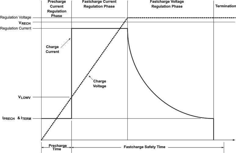 Figure 10. Typical Charging Profile
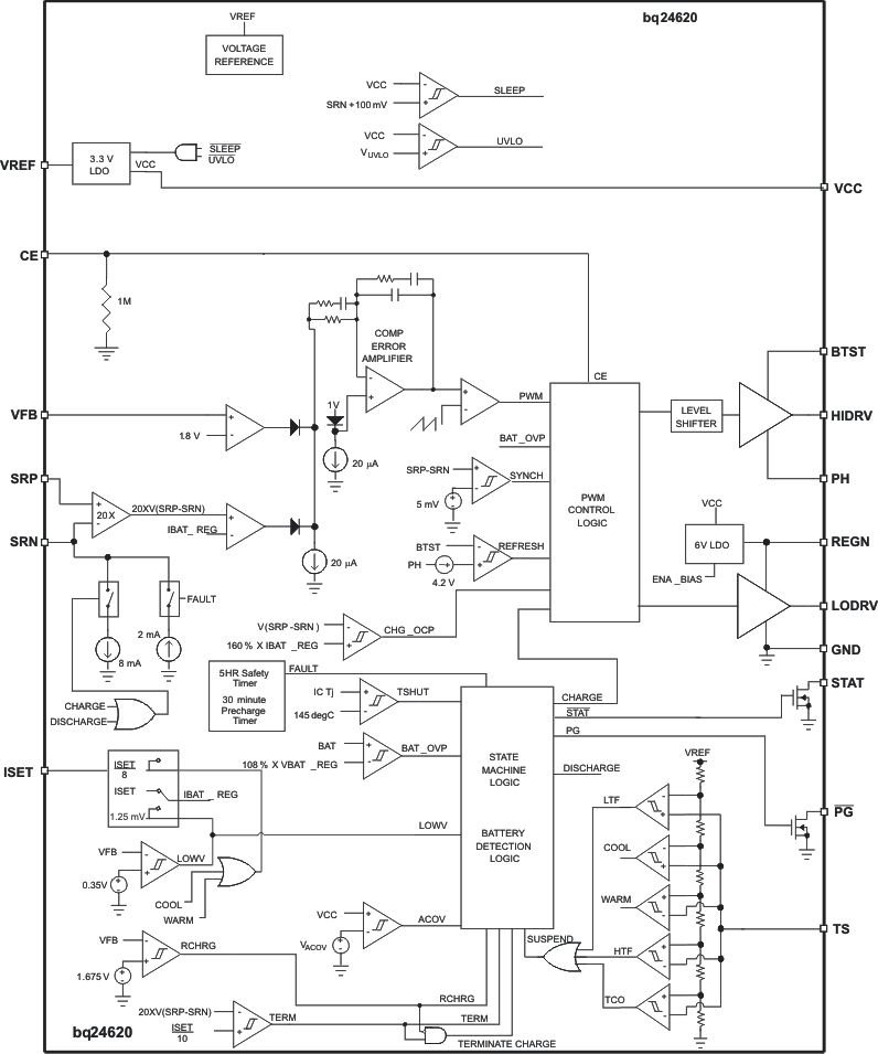
8.2 Functional Block Diagram
8.3 Feature Description
8.3.1 Battery Voltage Regulation
The bq24620 uses a high-accuracy voltage band gap and regulator for the charging voltage. The charge voltage is programmed through a resistor-divider from the battery to ground, with the midpoint tied to the VFB pin. The voltage at the VFB pin is regulated to 1.8 V, giving Equation 1 for the regulation voltage:

where
- where R2 is connected from VFB to the battery and R1 is connected from VFB to GND.
8.3.2 Battery Current Regulation
The ISET1 input sets the maximum charging current. Battery current is sensed by resistor RSR connected between SRP and SRN. The full-scale differential voltage between SRP and SRN is 100 mV. Thus, for a 10-mΩ sense resistor, the maximum charging current is 10 A. Equation 2 is for charge current:

VISET, the input voltage range of ISET, is from 0 to 2 V. The SRP and SRN pins are used to sense voltage across RSR with default value of 10 mΩ. However, resistors of other values can also be used. A larger sense resistor gives a larger sense voltage and a higher regulation accuracy, but at the expense of higher conduction loss.
8.3.3 Precharge
On power up, if the battery voltage is below the VLOWV threshold, the bq24620 applies 125 mA to the battery.
8.3.4 Charge Termination, Recharge, and Safety Timer
The bq24620 monitors the charging current during the voltage regulation phase. Termination is detected while the voltage on the VFB pin is higher than the VRECH threshold AND the charge current is less than the ITERM threshold, which is 1/10th of programmed charge current, as calculated in Equation 3:

As a safety backup, the bq24620 also provides an internal 5-hour charge timer for fast charge.
A new charge cycle is initiated when one of the following conditions occurs:
- The battery voltage falls below the recharge threshold.
- A power-on reset (POR) event occurs.
- CE is toggled.
8.3.5 Power Up
The bq24620 uses a SLEEP comparator to determine the source of power on the VCC pin, because VCC can be supplied either from the battery or the adapter. If the VCC voltage is greater than the SRN voltage, the bq24620 enables ACFET and disables BATFET. If all other conditions are met for charging, the bq24620 then attempts to charge the battery (see Enable and Disable Charging). If the SRN voltage is greater than VCC, indicating that the battery is the power source, bq24620 enters a low-quiescent-current (<15 μA) SLEEP mode to minimize current drain from the battery.
If VCC is below the UVLO threshold, the device is disabled.
8.3.6 Enable and Disable Charging
The following conditions must be valid before charge is enabled:
- CE is HIGH.
- The device is not in VCCLOWV mode.
- The device is not in SLEEP mode (that is, VCC > SRN) .
- The VCC voltage is lower than the ac overvoltage threshold (VCC < VACOV).
- 30-ms delay is complete after initial power up.
- The REGN LDO and VREF LDO voltages are at the correct levels.
- Thermal shutdown (TSHUT) is not valid.
- TS fault is not detected.
Any of the following conditions stops ongoing charging:
- CE is LOW.
- Adapter is removed, causing the device to enter VCCLOWV or SLEEP mode.
- Adapter voltage is less than 100 mV above battery.
- Adapter is over voltage.
- The REGN or VREF LDOs are overloaded.
- TSHUT IC temperature threshold is reached (145°C on rising edge with 15°C hysteresis).
- TS voltage goes out of range, indicating the battery temperature is too hot or too cold.
- Safety timer times out.
8.3.7 Automatic Internal Soft-Start Charger Current
The charger automatically soft-starts the charger regulation current every time the charger goes into fast-charge to ensure there is no overshoot or stress on the output capacitors or the power converter. The soft-start consists of stepping up the charge regulation current into eight evenly divided steps up to the programmed charge current. Each step lasts around 1.6 ms, for a typical rise time of 12.8 ms. No external components are needed for this function.
8.3.8 Converter Operation
The synchronous buck PWM converter uses a fixed-frequency voltage mode with a feed-forward control scheme. A type-III compensation network allows using ceramic capacitors at the output of the converter. The compensation input stage is connected internally between the feedback output (FBO) and the error amplifier input (EAI). The feedback compensation stage is connected between the error amplifier input (EAI) and error amplifier output (EAO). The LC output filter is selected to give a resonant frequency of 10 kHz to 15 kHz for bq24620, where the resonant frequency, fo, is given by:

An internal sawtooth ramp is compared to the internal EAO error control signal to vary the duty cycle of the converter. The ramp height is 7% of the input adapter voltage, making it always directly proportional to the input adapter voltage. This cancels out any loop gain variation due to a change in input voltage, and simplifies the loop compensation. The ramp is offset by 300 mV in order to allow zero-percent duty cycle when the EAO signal is below the ramp. The EAO signal is also allowed to exceed the sawtooth ramp signal in order to get a 100% duty-cycle PWM request. Internal gate-drive logic allows achieving 99.95% duty cycle while ensuring the N-channel upper device always has enough voltage to stay fully on. If the BTST pin to PH pin voltage falls below 4.2 V for more than three cycles, then the high-side N-channel power MOSFET is turned off and the low-side N-channel power MOSFET is turned on to pull the PH node down and recharge the BTST capacitor. Then the high-side driver returns to 100% duty-cycle operation until the (BTST–PH) voltage is detected to fall low again due to leakage current discharging the BTST capacitor below 4.2 V, and the reset pulse is reissued.
The fixed-frequency oscillator keeps tight control of the switching frequency under all conditions of input voltage, battery voltage, charge current, and temperature, simplifying output filter design and keeping it out of the audible noise region. Also see Application and Implementation for how to select the inductor, capacitor, and MOSFET.
8.3.9 Synchronous and Nonsynchronous Operation
The charger operates in synchronous mode when the SRP-SRN voltage is above 5 mV (0.5-A inductor current for a 10-mΩ sense resistor). During synchronous mode, the internal gate-drive logic ensures there is break-before-make complementary switching to prevent shoot-through currents. During the 30-ns dead time where both FETs are off, the body diode of the low-side power MOSFET conducts the inductor current. Having the low-side FET turn on keeps the power dissipation low, and allows safely charging at high currents. During synchronous mode, the inductor current is always flowing and the converter operates in continuous conduction mode (CCM), creating a fixed two-pole system.
The charger operates in nonsynchronous mode when the SRP-SRN voltage is below 5 mV (0.5-A inductor current for a 10-mΩ sense resistor). The charger is forced into nonsynchronous mode when the battery voltage is lower than 2 V or when the average SRP-SRN voltage is lower than 1.25 mV.
During nonsynchronous operation, the body diode of the low-side MOSFET can conduct the positive inductor current after the high-side N-channel power MOSFET turns off. When the load current decreases and the inductor current drops to zero, the body diode is naturally turned off and the inductor current becomes discontinuous. This mode is called discontinuous conduction mode (DCM). During DCM, the low-side N-channel power MOSFET turns on for around 80 ns when the bootstrap capacitor voltage drops below 4.2 V; then the low-side power MOSFET turns off and stays off until the beginning of the next cycle, where the high-side power MOSFET is turned on again. The 80-ns low-side MOSFET on-time is required to ensure the bootstrap capacitor is always recharged and able to keep the high-side power MOSFET on during the next cycle. This is important for battery chargers, where unlike regular DC-DC converters, there is a battery load that maintains a voltage and can both source and sink current. The 80-ns low-side pulse pulls the PH node (connection between high- and low-side MOSFETs) down, allowing the bootstrap capacitor to recharge up to the REGN LDO value. After the 80 ns, the low-side MOSFET is kept off to prevent negative inductor current from occurring.
At very low currents during nonsynchronous operation, there may be a small amount of negative inductor current during the 80-ns recharge pulse. The charge must be low enough to be absorbed by the input capacitance. Whenever the converter goes into zero-percent duty cycle, the high-side MOSFET does not turn on, and the low-side MOSFET does not turn on (only 80-ns recharge pulse) either, and there is almost no discharge from the battery.
During the DCM mode, the loop response automatically changes and has a single-pole system at which the pole is proportional to the load current, because the converter does not sink current, and only the load provides a current sink. This means at very low currents the loop response is slower, as there is less sinking current available to discharge the output voltage.
8.3.10 Cycle-by-Cycle Charge Undercurrent
If the SRP-SRN voltage decreases below 5 mV (the charger is also forced into nonsynchronous mode when the average SRP-SRN voltage is lower than 1.25 mV), the low-side FET is turned off for the remainder of the switching cycle to prevent negative inductor current. During DCM, the low-side FET only turns on for around 80 ns when the bootstrap capacitor voltage drops below 4.2 V to provide refresh charge for the bootstrap capacitor. This is important to prevent negative inductor current from causing a boost effect in which the input voltage increases as power is transferred from the battery to the input capacitors, which leads to an overvoltage stress on the VCC node and potentially causes damage to the system.
8.3.11 Input Overvoltage Protection (ACOV)
ACOV provides protection to prevent system damage due to high input voltage. Once the adapter voltage reaches the ACOV threshold, charge is disabled and the battery is switched to the system instead of the adapter.
8.3.12 Input Undervoltage Lockout (UVLO)
The system must have a minimum VCC voltage to allow proper operation. This VCC voltage could come from either input the adapter orthe battery, if a conduction path exists from the battery to VCC through the high-side NMOS body diode. When VCC is below the UVLO threshold, all circuits in the IC are disabled.
8.3.13 Battery Overvoltage Protection
The converter does not allow the high-side FET to turn on until the BAT voltage goes below 105% of the regulation voltage. This allows one-cycle response to an overvoltage condition, such as occurs when the load is removed or the battery is disconnected. An 8-mA current sink from SRP/SRN to PGND is on only during charge and allows discharging the stored output inductor energy that is transferred to the output capacitors. BATOVP also suspends the safety timer.
8.3.14 Cycle-by-Cycle Charge Overcurrent Protection
The charger has a secondary cycle-to-cycle overcurrent protection. The charger monitors the charge current, and prevents the current from exceeding 160% of the programmed charge current. The high-side gate drive turns off when the overcurrent is detected, and automatically resumes when the current falls below the overcurrent threshold.
8.3.15 Thermal Shutdown Protection
The QFN package has low thermal impedance, which provides good thermal conduction from the silicon to the ambient, to keep junctions temperatures low. As an added level of protection, the charger converter turns off and self-protects whenever the junction temperature exceeds the TSHUT threshold of 145°C. The charger stays off until the junction temperature falls below 130°C. Then the charger soft-starts again if all other enable-charge conditions are valid. Thermal shutdown also suspends the safety timer.
8.3.16 Temperature Qualification
The controller continuously monitors battery temperature by measuring the voltage between the TS pin and GND. A negative temperature coefficient thermistor (NTC) and an external voltage divider typically develop this voltage. The controller compares this voltage against its internal thresholds to determine if charging is allowed. To initiate a charge cycle, the battery temperature must be within the VLTF to VHTF thresholds. If battery temperature is outside of this range, the controller suspends charge and the safety timer and waits until the battery temperature is within the VLTF to VHTF range. During the charge cycle, the battery temperature must be within the VLTF to VTCO thresholds. If the battery temperature is outside of this range, the controller suspends charge and the safety timer and waits until the battery temperature is within the VLTF to VHTF range. If the battery temperature is between the VLTF and VCOOL thresholds or between the VHTF and VWARM thresholds, charge is automatically reduced to ICHARGE/8. To avoid early termination during COOL/WARM condition, set ITERM ≤ ICHARGE/10. The controller suspends charge by turning off the PWM charge FETs. Figure 11 and Figure 12 summarize the operation.
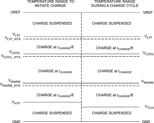 Figure 11. TS, Thermistor Sense Thresholds
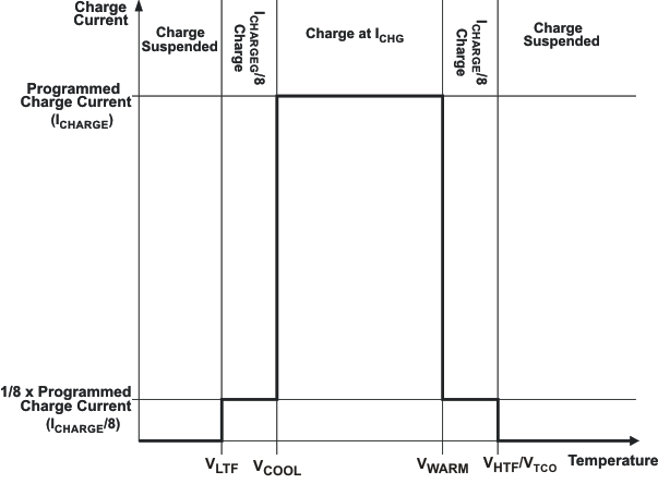 Figure 12. Typical Charge Current vs Temperature Profile
Assuming a 103AT NTC thermistor on the battery pack as shown in Figure 17, the values of RT1 and RT2 can be determined by using Equation 5 and Equation 6:


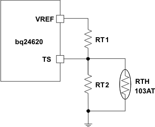 Figure 13. TS Resistor Network
For example, a 103AT NTC thermistor is used to monitor the battery pack temperature. Select TCOOL = 0ºC, TWARM = 60ºC. From the calculation and selecting a standard 5% resistor value, we can get RT1 = 2.2 kΩ, RT2 = 6.8 kΩ, and TCOLD is –17ºC (target –20ºC); THOT is 77ºC (target 75ºC), and TCUT-OFF is 86ºC (target 80ºC). A small RC filter is suggested to protect the TS pin from system-level ESD.
8.3.17 Timer Fault Recovery
The bq24620 provides a recovery method to deal with timer fault conditions. The following summarizes this method:
Condition 1: The battery voltage is above the recharge threshold and a time-out fault occurs.
Recovery Method: The timer fault clears when the battery voltage falls below the recharge threshold, and battery detection begins. Taking CE low, or a POR condition, also clears the fault.
Condition 2: The battery voltage is below the RECHARGE threshold and a time-out fault occurs.
Recovery Method: Under this scenario, the bq24620 applies the IFAULT current to the battery. This small current is used to detect a battery removal condition and remains on as long as the battery voltage stays below the recharge threshold. If the battery voltage goes above the recharge threshold, the bq24620 disables the fault current and executes the recovery method described in Condition 1. Taking CE low, or a POR condition, also clears the fault.
8.3.18 PG Output
The open-drain PG (power good) indicates whether the VCC voltage is valid or not. The open-drain FET turns on whenever the bq24620 has a valid VCC input (not in UVLO or ACOV or SLEEP mode). The PG pin can be used to drive an LED or communicate with the host processor.
8.3.19 CE (Charge Enable)
The CE digital input is used to disable or enable the charge process. A high-level signal on this pin enables charge, provided all the other conditions for charge are met (see Enable and Disable Charging). A high-to-low transition on this pin also resets all timers and fault conditions. There is an internal 1-MΩ pulldown resistor on the CE pin, so if CE is floated, the charge does not turn on.
8.3.20 Charge Status Outputs
The open-drain STAT outputs indicate various charger operations as shown in Table 2. These status pins can be used to drive LEDs or communicate with the host processor. OFF indicates that the open-drain transistor is turned off.
Table 2. Stat Pin Definition For Bq24620
| CHARGE STATE | STAT |
|---|---|
| Charge in progress | ON |
| Charge complete (PG = LOW) | OFF |
| Sleep mode (PG = HIGH) | OFF |
| Charge suspend, timer fault, ACOV, battery absent | BLINK (0.5 Hz) |
8.3.21 Battery Detection
For applications with removable battery packs, the bq24620 provides a battery-absent detection scheme to reliably detect insertion or removal of battery packs. CE must be HIGH to enable battery detection function.
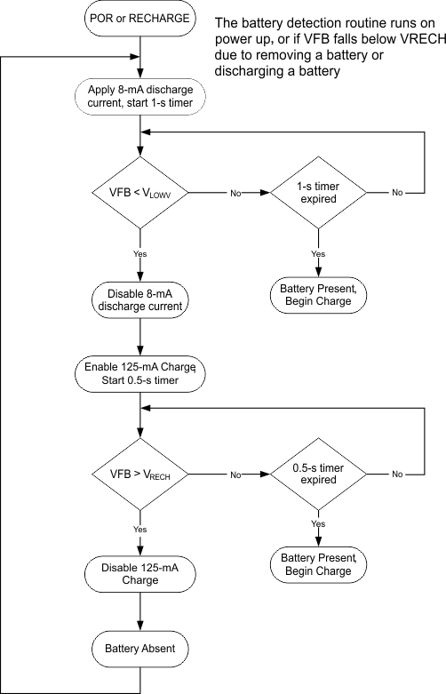 Figure 14. Battery Detection Flow Chart
Once the device has powered up, an 8-mA discharge current is applied to the SRN terminal. If the battery voltage falls below the LOWV threshold within 1 second, the discharge source is turned off, and the charger is turned on at low charge current (125 mA). If the battery voltage rises above the recharge threshold within 500 ms, no battery is present and the cycle restarts. If either the 500-ms or 1-second timer times out before the respective thresholds are hit, a battery is detected and a charge cycle is initiated. See Maximum Output Capacitance for more information.
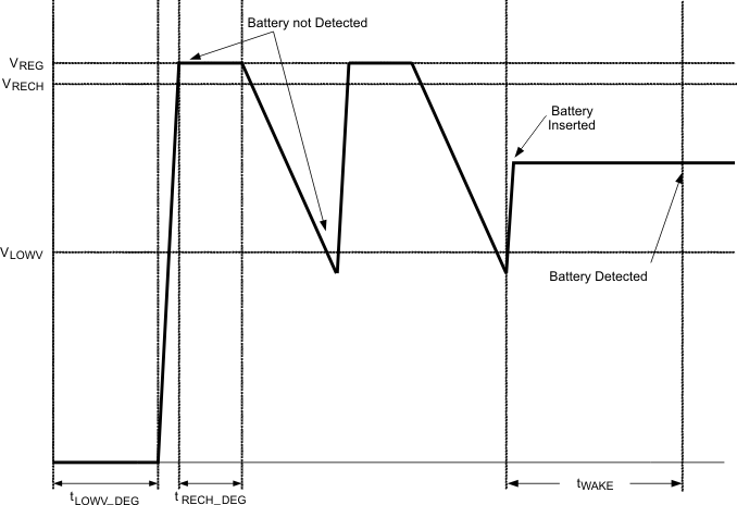 Figure 15. Battery-Detect Timing Diagram
8.4 Device Functional Modes
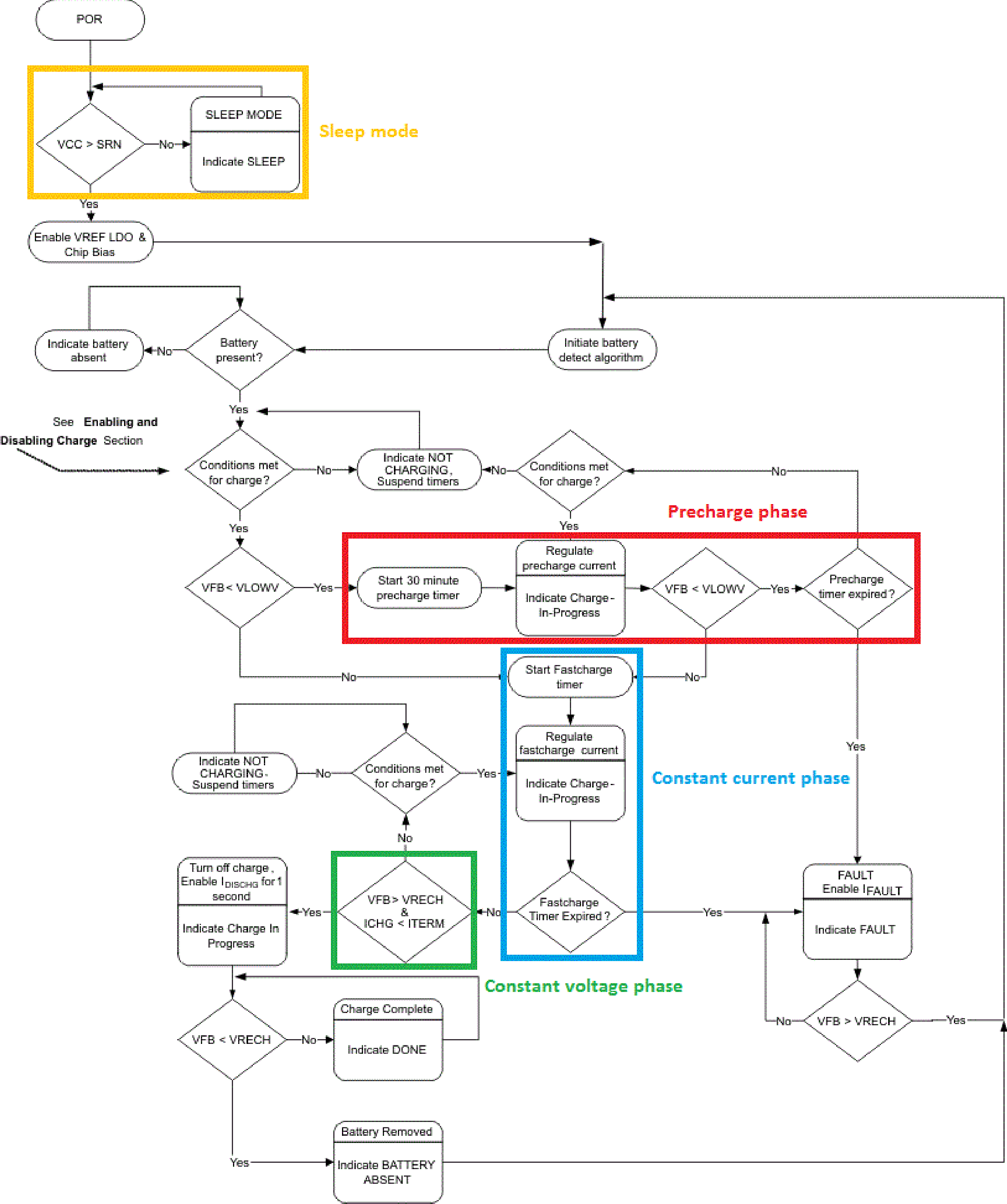 Figure 16. Device Operational Flow Chart