SLUSEG2C
September 2022 ā February 2024
BQ25620
,
BQ25622
PRODUCTION DATA
1
1
Features
2
Applications
3
Description
4
Description (continued)
5
Device Comparison
6
Pin Configuration and Functions
7
Specifications
7.1
Absolute Maximum Ratings
7.2
ESD Ratings
7.3
Recommended Operating Conditions
7.4
Thermal Information
7.5
Electrical Characteristics
7.6
Timing Requirements
7.7
Typical Characteristics
8
Detailed Description
8.1
Overview
8.2
Functional Block Diagram
8.3
Feature Description
8.3.1
Power-On-Reset (POR)
8.3.2
Device Power Up from Battery
8.3.3
Device Power Up from Input Source
8.3.3.1
REGN LDO Power Up
8.3.3.2
Poor Source Qualification
8.3.3.3
D+/Dā Detection Sets Input Current Limit (BQ25620 Only)
8.3.3.4
ILIM Pin (BQ25622 Only)
8.3.3.5
Input Voltage Limit Threshold Setting (VINDPM Threshold)
8.3.3.6
Converter Power-Up
8.3.4
Power Path Management
8.3.4.1
Narrow VDC Architecture
8.3.4.2
Dynamic Power Management
8.3.4.3
High Impedance Mode
8.3.5
Battery Charging Management
8.3.5.1
Autonomous Charging Cycle
8.3.5.2
Battery Charging Profile
8.3.5.3
Charging Termination
8.3.5.4
Thermistor Qualification
8.3.5.4.1
Advanced Temperature Profile in Charge Mode
8.3.5.4.2
TS Pin Thermistor Configuration
8.3.5.4.3
Cold/Hot Temperature Window in OTG Mode
8.3.5.4.4
JEITA Charge Rate Scaling
8.3.5.4.5
TS_BIAS Pin (BQ25622 Only)
8.3.5.5
Charging Safety Timers
8.3.6
USB On-The-Go (OTG)
8.3.6.1
Boost OTG Mode
8.3.7
Integrated 12-Bit ADC for Monitoring
8.3.8
Status Outputs ( PG, STAT, INT)
8.3.8.1
PG Pin Power Good Indicator
8.3.8.2
Interrupts and Status, Flag and Mask Bits
8.3.8.3
Charging Status Indicator (STAT)
8.3.8.4
Interrupt to Host ( INT)
8.3.9
BATFET Control
8.3.9.1
Shutdown Mode
8.3.9.2
Ship Mode
8.3.9.3
System Power Reset
8.3.10
Protections
8.3.10.1
Voltage and Current Monitoring in Battery Only and HIZ Modes
8.3.10.1.1
Battery Undervoltage Lockout
8.3.10.1.2
Battery Overcurrent Protection
8.3.10.2
Voltage and Current Monitoring in Buck Mode
8.3.10.2.1
Input Overvoltage
8.3.10.2.2
System Overvoltage Protection (SYSOVP)
8.3.10.2.3
Forward Converter Cycle-by-Cycle Current Limit
8.3.10.2.4
System Short
8.3.10.2.5
Battery Overvoltage Protection (BATOVP)
8.3.10.2.6
Sleep and Poor Source Comparators
8.3.10.3
Voltage and Current Monitoring in Boost Mode
8.3.10.3.1
Boost Mode Overvoltage Protection
8.3.10.3.2
Boost Mode Duty Cycle Protection
8.3.10.3.3
Boost Mode PMID Undervoltage Protection
8.3.10.3.4
Boost Mode Battery Undervoltage
8.3.10.3.5
Boost Converter Cycle-by-Cycle Current Limit
8.3.10.3.6
Boost Mode SYS Short
8.3.10.4
Thermal Regulation and Thermal Shutdown
8.3.10.4.1
Thermal Protection in Buck Mode
8.3.10.4.2
Thermal Protection in Boost Mode
8.3.10.4.3
Thermal Protection in Battery-Only Mode
8.4
Device Functional Modes
8.4.1
Host Mode and Default Mode
8.4.2
Register Bit Reset
8.5
Programming
8.5.1
Serial Interface
8.5.1.1
Data Validity
8.5.1.2
START and STOP Conditions
8.5.1.3
Byte Format
8.5.1.4
Acknowledge (ACK) and Not Acknowledge (NACK)
8.5.1.5
Target Address and Data Direction Bit
8.5.1.6
Single Write and Read
8.5.1.7
Multi-Write and Multi-Read
8.6
Register Maps
8.6.1
Register Programming
8.6.2
BQ25620 Registers
9
Application and Implementation
9.1
Application Information
9.2
Typical Application
9.2.1
Design Requirements
9.2.2
Detailed Design Procedure
9.2.2.1
Inductor Selection
9.2.2.2
Input Capacitor
9.2.2.3
Output Capacitor
9.2.3
Application Curves
10
Power Supply Recommendations
11
Layout
11.1
Layout Guidelines
11.2
Layout Example
12
Device and Documentation Support
12.1
Device Support
12.1.1
Third-Party Products Disclaimer
12.2
Documentation Support
12.2.1
Related Documentation
12.3
Receiving Notification of Documentation Updates
12.4
Support Resources
12.5
Trademarks
12.6
Electrostatic Discharge Caution
12.7
Glossary
13
Revision History
14
Mechanical, Packaging, and Orderable Information
Package Options
Mechanical Data (Package|Pins)
RYK|18
MPQF634
Thermal pad, mechanical data (Package|Pins)
Orderable Information
sluseg2c_oa
sluseg2c_pm
11.2
Layout Example
Figure 11-1
High Frequency Current Path
Figure 11-2
Layout Example: Top Layer (red) and All PGND Internal Layer 2 (brown)
Figure 11-3
Layout Example: Inner Layer 3 (AGND pour; SW node pour; signal routing)
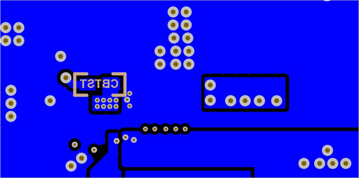
Figure 11-4
Layout Example: Bottom Layer X-Ray From Top (PGND pour; BTST capacitor; redundant SW, SYS and BAT pours)