SLVSDU0B September 2017 – September 2019 BQ25910
PRODUCTION DATA.
- 1 Features
- 2 Applications
- 3 Description
- 4 Revision History
- 5 Pin Configuration and Functions
- 6 Specifications
-
7 Detailed Description
- 7.1 Overview
- 7.2 Functional Block Diagram
- 7.3
Feature Description
- 7.3.1 Device Power-On-Reset (POR)
- 7.3.2 Device Power Up from Battery without Input Source
- 7.3.3 Device Power Up from Input Source
- 7.3.4 Power Up REGN LDO
- 7.3.5 Poor Source Qualification
- 7.3.6 Converter Power-Up
- 7.3.7 Three-Level Buck Converter Theory of Operation
- 7.3.8 Host Mode and Default Mode
- 7.3.9 Battery Charging Management
- 7.3.10 Master Charger and Parallel Charger Interactions
- 7.3.11 Battery Charging Profile
- 7.4 Device Functional Modes
- 7.5 Programming
- 7.6
Register Maps
- 7.6.1
I2C Registers
- 7.6.1.1 Battery Voltage Regulation Limit Register (Address = 0h) [reset = AAh]
- 7.6.1.2 Charger Current Limit Register (Address = 1h) [reset = 46h]
- 7.6.1.3 Input Voltage Limit Register (Address = 2h) [reset = 04h]
- 7.6.1.4 Input Current Limit Register (Address = 3h) [reset = 13h]
- 7.6.1.5 Reserved Register (Address = 4h) [reset = 03h]
- 7.6.1.6 Charger Control 1 Register (Address = 5h) [reset = 9Dh]
- 7.6.1.7 Charger Control 2 Register (Address = 6h) [reset = 33h]
- 7.6.1.8 INT Status Register (Address = 7h) [reset = X]
- 7.6.1.9 FAULT Status Register (Address = 8h) [reset = X]
- 7.6.1.10 INT Flag Status Register (Address = 9h) [reset = 00h]
- 7.6.1.11 FAULT Flag Register (Address = Ah) [reset = 00h]
- 7.6.1.12 INT Mask Register (Address = Bh) [reset = 00h]
- 7.6.1.13 FAULT Mask Register (Address = Ch) [reset = 00h]
- 7.6.1.14 Part Information Register (Address = Dh) [reset = 0Ah]
- 7.6.1
I2C Registers
- 8 Application and Implementation
- 9 Power Supply Recommendations
- 10Layout
- 11Device and Documentation Support
- 12Mechanical, Packaging, and Orderable Information
Package Options
Refer to the PDF data sheet for device specific package drawings
Mechanical Data (Package|Pins)
- YFF|36
Thermal pad, mechanical data (Package|Pins)
Orderable Information
8.2.2.4 Flying Capacitor
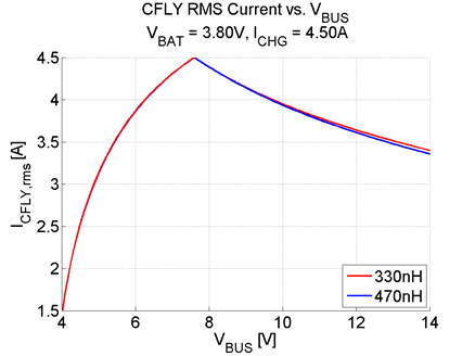
Flying capacitor selection must meet criteria related to current ripple and voltage ripple. Just as the input capacitor, the flying capacitor should also have enough ripple current rating to absorb the RMS current through it:

This function becomes maximum when D = 0.5, because at that point the capacitor is in series with the inductor for a complete switching cycle, and their RMS currents are the same. The flying capacitor should be sized to handle the full charge current in the scenario where D = 0.5.
 Figure 47. Flying Capacitor RMS Current vs. VBUS with Fixed VBAT and ICHG
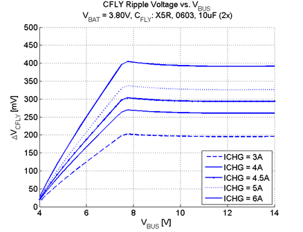
 Additionally, the flying capacitor voltage ripple should be kept under 10% of VBUS/2 to ensure loop stability. This quantity is given by the following equation:

It is recommended to use at least two 16-V, 10-μF, low ESR ceramic capacitors in parallel to achieve both RMS current rating and maintain voltage ripple <10% in the flying capacitor for up-to 6-A charge current application. The following curve shows what the ripple voltage of CFLY might look like for such a configuration by taking into account voltage derating of the capacitor and plugging the effective capacitance value into equation above at different charge currents and VBUS voltages.
 Figure 48. Flying Capacitor Ripple Voltage vs. VBUS with Fixed VBAT
 Table 22. Recommended CFLY Values
| CHARGE CURRENT | CFLY CONFIGURATION |
|---|---|
| ICHG < 3.5 A | 1 x 0603 (10 μF, X5R, 16 V) |
| ICHG > 3.5 A | 2 x 0603 (10 μF, X5R, 16 V) |