SLUSAJ3K September 2011 – August 2022 BQ294502 , BQ294504 , BQ294506 , BQ294512 , BQ294522 , BQ294524 , BQ294532 , BQ294533 , BQ294534 , BQ294582 , BQ294592
PRODUCTION DATA
- 1 Features
- 2 Applications
- 3 Description
- 4 Revision History
- 5 Device Comparison Table
- 6 Pin Configuration and Functions
- 7 Specifications
- 8 Detailed Description
- 9 Application and Implementation
- 10Power Supply Recommendations
- 11Layout
- 12Device and Documentation Support
- 13Mechanical, Packaging, and Orderable Information
Package Options
Mechanical Data (Package|Pins)
- DRV|6
Thermal pad, mechanical data (Package|Pins)
- DRV|6
Orderable Information
8.3 Feature Description
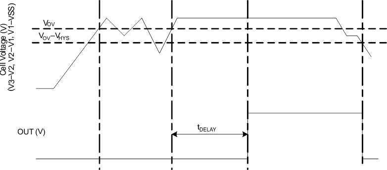
The voltage sensing for each cell is done independently using a multiplexer. The method of overvoltage detection is comparing the voltage to an overvoltage protection voltage VOV. Once the voltage exceeds the programmed fixed value, the delay timer circuit is activated. This delay (tDELAY) is fixed for either a 4-s or 6.5-s delay. When these conditions are satisfied, the OUT terminal is transitioned to a high level. This output (OUT) is released to a low condition if all of the cell inputs (Vx) are below the OVP threshold minus the Vhys.
 Figure 8-1 Timing for Overvoltage Sensing