SLUSAJ3K September 2011 – August 2022 BQ294502 , BQ294504 , BQ294506 , BQ294512 , BQ294522 , BQ294524 , BQ294532 , BQ294533 , BQ294534 , BQ294582 , BQ294592
PRODUCTION DATA
- 1 Features
- 2 Applications
- 3 Description
- 4 Revision History
- 5 Device Comparison Table
- 6 Pin Configuration and Functions
- 7 Specifications
- 8 Detailed Description
- 9 Application and Implementation
- 10Power Supply Recommendations
- 11Layout
- 12Device and Documentation Support
- 13Mechanical, Packaging, and Orderable Information
Package Options
Mechanical Data (Package|Pins)
- DRV|6
Thermal pad, mechanical data (Package|Pins)
- DRV|6
Orderable Information
3 Description
The BQ2945xy family of products is a secondary-level voltage monitor and protector for Li-ion battery pack systems. Each cell is monitored independently for an overvoltage condition. Based on the configuration, an output is triggered after a fixed delay if any of the two or three cells has an overvoltage condition. This output is triggered into a high state after an overvoltage condition satisfies the specified delay timer.
Device
Information
| PART NUMBER(1) | PACKAGE | BODY SIZE (NOM) |
|---|---|---|
| BQ2945xy | SON (6) | 2.00 mm × 2.00 mm |
(1) For all available packages, see the orderable addendum at the end of
the data sheet.
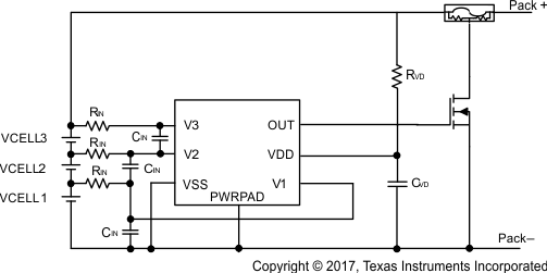
 Simplified Schematic