SLUSBV4B June 2018 – September 2020 BQ40Z80
PRODUCTION DATA
- 1 Features
- 2 Applications
- 3 Description
- 4 Revision History
- 5 Description (continued)
- 6 Pin Configuration and Functions
- 7 Specifications
-
8 Detailed Description
- 8.1 Overview
- 8.2 Functional Block Diagram
- 8.3
Feature Description
- 8.3.1 Primary (1st Level) Safety Features
- 8.3.2 Secondary (2nd Level) Safety Features
- 8.3.3 Charge Control Features
- 8.3.4 Gas Gauging
- 8.3.5 Multifunction Pins
- 8.3.6 Configuration
- 8.3.7 Battery Parameter Measurements
- 8.3.8 Lifetime Data Logging Features
- 8.3.9 Authentication
- 8.3.10 LED Display
- 8.3.11 IATA Support
- 8.3.12 Voltage
- 8.3.13 Current
- 8.3.14 Temperature
- 8.3.15 Communications
- 8.4 Device Functional Modes
- 9 Applications and Implementation
- 10Power Supply Recommendations
- 11Layout
- 12Device and Documentation Support
- 13Mechanical, Packaging, and Orderable Information
Package Options
Mechanical Data (Package|Pins)
- RSM|32
Thermal pad, mechanical data (Package|Pins)
- RSM|32
Orderable Information
Pin Functions
| PIN | TYPE | DESCRIPTION | |
|---|---|---|---|
| NAME | NUMBER | ||
| VC5 | 1 | AI(1) | Sense voltage input pin for the fifth cell from the bottom of the stack, balance current input for the fifth cell from the bottom of the stack, and return balance current for the sixth cell from the bottom of the stack. Should be connected to the positive terminal of the fifth cell from the bottom of stack with a 100-Ω series resistor and a 0.1-µF capacitor to VC4. If not used, connect to VC4. |
| VC4 | 2 | AI | Sense voltage input pin for the fourth cell from the bottom of the stack, balance current input for the fourth cell from the bottom of the stack, and return balance current for the fifth cell from the bottom of the stack. Should be connected to the positive terminal of the fourth cell from the bottom of stack with a 100-Ω series resistor and a 0.1-µF capacitor to VC3. If not used, connect to VC3. |
| VC3 | 3 | AI | Sense voltage input pin for the third cell from the bottom of the stack, balance current input for the third cell from the bottom of the stack, and return balance current for the fourth cell from the bottom of the stack. Should be connected to the positive terminal of the third cell from the bottom of stack with a 100-Ω series resistor and a 0.1-µF capacitor to VC2. If not used, connect to VC2. |
| VC2 | 4 | AI | Sense voltage input pin for the second cell from the bottom of the stack, balance current input for the second cell from the bottom of the stack, and return balance current for the third cell from the bottom of the stack. Should be connected to the positive terminal of the second cell from the bottom of stack with a 100-Ω series resistor and a 0.1-µF capacitor to VC1. If not used, connect to VC1. |
| VC1 | 5 | AI | Sense voltage input pin for the first cell from the bottom of the stack, balance current input for the first cell from the bottom of the stack, and return balance current for the second cell from the bottom of the stack. Should be connected to the positive terminal of the first cell from the bottom of stack with a 100-Ω series resistor and a 0.1-µF capacitor to VSS. |
| SRN | 6 | I | Analog input pin connected to the internal coulomb counter peripheral for integrating a small voltage between SRP and SRN, where SRP is the top of the sense resistor and charging current flows from SRP to SRN. Should be connected through an RC filter to the sense resistor terminal connected to PACK– (not CELL–). |
| NC | 7 | — | Not internally connected |
| SRP | 8 | I | Analog input pin connected to the internal coulomb counter peripheral for integrating a small voltage between SRP and SRN, where SRP is the top of the sense resistor and charging current flows from SRP to SRN. Should be connected through an RC filter to the sense resistor positive terminal, which is connected to the least-positive cells negative terminal. |
| VSS | 9 | P | Device ground |
| TS1 | 10 | AI | Temperature sensor 1 thermistor input pin. Connect to thermistor-1. If not used, connect directly to VSS and configure data flash accordingly. |
| TS2 | 11 | AI | Temperature sensor 2 thermistor input pin. Connect to thermistor-2. If not used, connect directly to VSS and configure data flash accordingly. |
| TS3/ADCIN1/ GPIO |
12 | IO | Multifunction pin for TS3, ADCIN1, and GPIO. Can be configured in
the control registers. If not used, connect directly to VSS and configure data flash
accordingly. TS3: Temperature sensor 3 thermistor input pin. Connect to thermistor-3. ADCIN1: General-purpose ADCIN pin. Connect properly scaled input to this pin. GPIO: Customizable GPIO |
| DISP/TS4/ADCIN2/GPIO | 13 | IO | Multifunction pin for the display button, temperature sensor
input, ADC input, or GPIO. Can be configured in the control registers. If not used,
connect directly to VSS and configure data flash accordingly. DISP: Connect to the display button or LED. TS4: Temperature sensor 4 thermistor input pin. Connect to thermistor-4. ADCIN2: General-purpose ADCIN pin. Connect properly scaled input to this pin. GPIO: Customizable GPIO |
| NC | 14 | — | Not internally connected |
| DISP/GPIO | 15 | I/OD | Multifunction pin for the display button, or GPIO. Can be
configured in the control registers. If not used, connect directly to VSS and
configure data flash accordingly. DISP: Connect to the display button or LED. GPIO: Customizable GPIO |
| PDSG/GPIO | 16 | I/OD | Multifunction pin for pre-discharge FET control, or GPIO. Can be
configured in the control registers. If not used, connect directly to VSS and
configure data flash accordingly. PDSG: Connect to the N-CH FET to control PRE-DISCHARGE mode. GPIO: Customizable GPIO |
| PRES/ SHUTDN/
DISP/ PDSG/GPIO |
17 | I/OD | Multifunction pin for host system present input, emergency system
shutdown, LED button control, pre-discharge control, or GPIO. Can be configured in
the control registers. If not used, connect directly to VSS and configure data flash
accordingly. PRES: Connect to host to detect system present input for a removable battery pack. Do not pullup this pin. SHUTDN: Emergency shutdown input for an embedded battery pack DISP: Connect to the display button or LED. PDSG: Connect to the N-CH FET to control PRE-DISCHARGE mode. GPIO: Customizable GPIO |
| SMBD | 18 | I/OD | SMBus data pin |
| SMBC | 19 | I/OD | SMBus clock pin |
| LEDCNTLA/PDSG/GPIO | 20 | O | Multifunction pin for LED display, pre-discharge, or GPIO. If not
used, connect to VSS with a 20-kΩ resistor. LEDCNTLA: LED display segment that drives the external LEDs, depending on the firmware configuration. PDSG: Connect to the N-CH FET to control PRE-DISCHARGE mode. GPIO: Customizable GPIO |
| LEDCNTLB/GPIO | 21 | O | Multifunction pin for LED display or GPIO. If not used, connect to
VSS with a 20-kΩ resistor. LEDCNTLB: LED display segment that drives the external LEDs, depending on the firmware configuration. GPIO: Customizable GPIO |
| LEDCNTLC/GPIO | 22 | O | Multifunction pin for LED display or GPIO. If not used, connect to
VSS with a 20-kΩ resistor. LEDCNTLC: LED display segment that drives the external LEDs, depending on the firmware configuration GPIO: Customizable GPIO |
| FUSE | 23 | O | Fuse drive output pin. Can be OR'ed together into the fuse N-CH FET gate drive with secondary protector. If not used, connect directly to VSS. |
| VCC | 24 | P | Secondary power supply input. Connect to the middle of protection FETs through the series resistor. |
| PACK | 25 | AI | Pack sense input pin. Connect through the series resistor to PACK+. |
| DSG | 26 | O | NMOS discharge FET drive output pin. Connect to the DSG FET gate. |
| NC | 27 | — | Not internally connected. |
| PCHG | 28 | O | PMOS precharge FET drive output pin. Connect to the PCHG FET gate if the precharge function is used. Leave floating if not used. |
| CHG | 29 | O | NMOS charge FET drive output pin. Connect to the CHG FET gate. |
| BAT | 30 | P | Primary power supply input pin. Connect through the diode and series resistor to the top of the cell stack. |
| PBI | 31 | P | Power supply backup input pin. Connect to the 2.2-µF capacitor to VSS. |
| VC6 | 32 | AI | Sense voltage input pin for the sixth cell from the bottom of the stack, balance current input for the sixth cell from the bottom of the stack. Should be connected to the positive terminal of the sixth cell from the bottom of stack with 100-Ω series resistor and a 0.1-µF capacitor to VC5. If not used, connect to VC5. |
(1) P = Power Connection, O = Digital Output, AI = Analog Input, I =
Digital Input, I/OD = Digital Input/Output
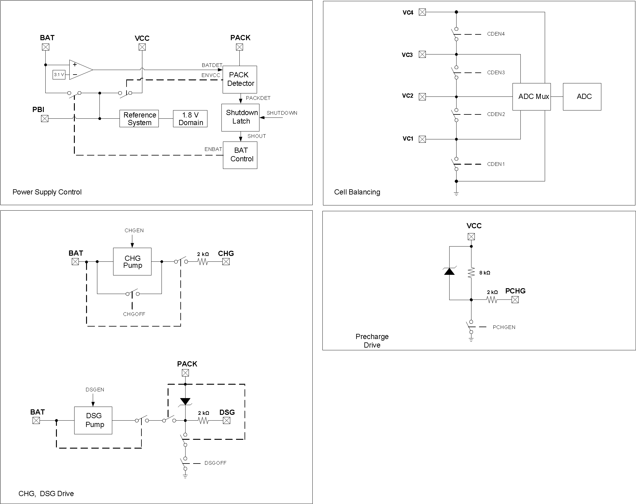
 Figure 6-2 Pin Equivalent
Diagram 1
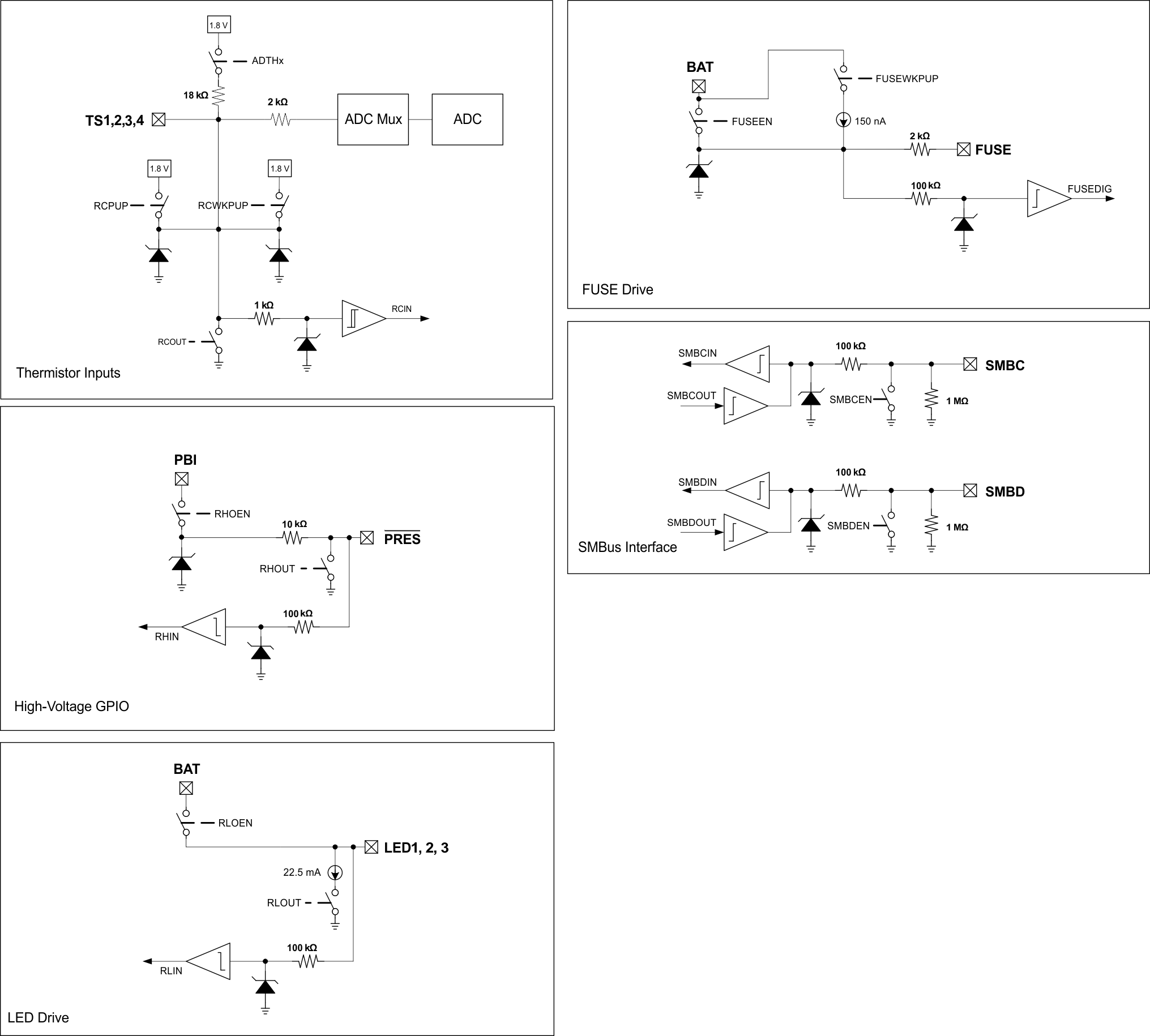
 Figure 6-3 Pin Equivalent
Diagram 2