SLUSFJ0A June 2024 – September 2024 BQ51013C-Q1
PRODUCTION DATA
- 1
- 1 Features
- 2 Applications
- 3 Description
- 4 Description (continued)
- 5 Device Comparison Table
- 6 Pin Configuration and Functions
- 7 Specifications
-
8 Detailed Description
- 8.1 Overview
- 8.2 Functional Block Diagram
- 8.3
Feature Description
- 8.3.1 Details of a Qi Wireless Power System and BQ51013C-Q1 Power Transfer Flow Diagrams
- 8.3.2 Dynamic Rectifier Control
- 8.3.3 Dynamic Efficiency Scaling
- 8.3.4 RILIM Calculations
- 8.3.5 Input Overvoltage
- 8.3.6 Adapter Enable Functionality and EN1/EN2 Control
- 8.3.7 End Power Transfer Packet (WPC Header 0x02)
- 8.3.8 Status Outputs
- 8.3.9 WPC Communication Scheme
- 8.3.10 Communication Modulator
- 8.3.11 Adaptive Communication Limit
- 8.3.12 Synchronous Rectification
- 8.3.13 Temperature Sense Resistor Network (TS)
- 8.3.14 3-State Driver Recommendations for the TS/CTRL Pin
- 8.3.15 Thermal Protection
- 8.3.16 WPC v2.0 Compliance – Foreign Object Detection
- 8.3.17 Receiver Coil Load-Line Analysis
- 8.4 Device Functional Modes
-
9 Application and Implementation
- 9.1 Application Information
- 9.2
Typical Applications
- 9.2.1
BQ51013C-Q1 Wireless Power Receiver Used as a Power
Supply
- 9.2.1.1 Design Requirements
- 9.2.1.2
Detailed Design Procedure
- 9.2.1.2.1 Using The BQ51013C-Q1 as a Wireless Power Supply: (See Figure 1-1 )
- 9.2.1.2.2 Series and Parallel Resonant Capacitor Selection
- 9.2.1.2.3 Recommended RX Coils
- 9.2.1.2.4 COMM, CLAMP, and BOOT Capacitors
- 9.2.1.2.5 Control Pins and CHG
- 9.2.1.2.6 Current Limit and FOD
- 9.2.1.2.7 RECT and OUT Capacitance
- 9.2.1.3 Application Curves
- 9.2.2 Dual Power Path: Wireless Power and DC Input
- 9.2.3 Wireless and Direct Charging of a Li-Ion Battery at 800 mA
- 9.2.1
BQ51013C-Q1 Wireless Power Receiver Used as a Power
Supply
- 10Power Supply Recommendations
- 11Layout
- 12Device and Documentation Support
- 13Revision History
- 14Mechanical, Packaging, and Orderable Information
Package Options
Refer to the PDF data sheet for device specific package drawings
Mechanical Data (Package|Pins)
- RHL|20
Thermal pad, mechanical data (Package|Pins)
- RHL|20
Orderable Information
9.2.1.2.2 Series and Parallel Resonant Capacitor Selection
Shown in Figure 9-1, the capacitors C1 (series) and C2 (parallel) make up the dual resonant circuit with the receiver coil. These two capacitors must be sized correctly per the WPC v2.0 specification. Figure 9-2 illustrates the equivalent circuit of the dual resonant circuit:
 Figure 9-2 Dual Resonant Circuit With the Receiver Coil
The Power Receiver Design Requirements in Volume 1 of the WPC v2.0 specification highlights in detail the sizing requirements. To summarize, the receiver designer will be required to take inductance measurements with a standard test fixture as shown in Figure 9-3:
") Figure 9-3 WPC v2.0 Receiver Coil
Test Fixture For the Inductance Measurement Ls’ (Copied From System Description
Wireless Power Transfer, Volume 1: Low Power, Part 1 Interface Definition,
Version 1.1)
Figure 9-3 WPC v2.0 Receiver Coil
Test Fixture For the Inductance Measurement Ls’ (Copied From System Description
Wireless Power Transfer, Volume 1: Low Power, Part 1 Interface Definition,
Version 1.1)The primary shield is to be 50 mm × 50 mm × 1 mm of Ferrite material PC44 from TDK Corp. The gap dZ is to be 3.4 mm. The receiver coil, as it will be placed in the final system (for example, the back cover and battery must be included if the system calls for this), is to be placed on top of this surface and the inductance is to be measured at 1-V RMS and a frequency of 100 kHz. This measurement is termed Ls’. The same measurement is to be repeated without the test fixture shown in Figure 9-3. This measurement is termed Ls or the free-space inductance. Each capacitor can then be calculated using Equation 6:
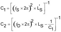
where
- fS is 100 kHz +5/-10%.
- fD is 1 MHz ±10%.
C1 must be chosen first prior to calculating C2.
The quality factor must be greater than 77 and can be determined by Equation 7:
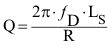
where
- R is the DC resistance of the receiver coil.
All other constants are defined above.
For this application, the selected coil inductance, Ls, is 11 µH and the Ls' is 16 µH with a DC resistance of 191 mΩ. Using Equation 6, the C1 resolves to 158.3 nF (with a range of 144 nF to 175 nF). For an optimum solution of 3 capacitors in parallel, the chosen capacitors are 68 nF, 47 nF, and 39 nF for a total of 154 nF, well within the desired range. Using the same equation (and the chosen value for C1), C2 resolves to 2.3 nF. This is easily met with capacitors of 2.2 nF and 100 pF. The C1 and C2 capacitors must have a minimum voltage rating of 25 V. Solving for the quality factor (Q in Equation 7), gives a value of over 500.
Table 9-1 lists the recommended RX coils.