SLUSFJ0A June 2024 – September 2024 BQ51013C-Q1
PRODUCTION DATA
- 1
- 1 Features
- 2 Applications
- 3 Description
- 4 Description (continued)
- 5 Device Comparison Table
- 6 Pin Configuration and Functions
- 7 Specifications
-
8 Detailed Description
- 8.1 Overview
- 8.2 Functional Block Diagram
- 8.3
Feature Description
- 8.3.1 Details of a Qi Wireless Power System and BQ51013C-Q1 Power Transfer Flow Diagrams
- 8.3.2 Dynamic Rectifier Control
- 8.3.3 Dynamic Efficiency Scaling
- 8.3.4 RILIM Calculations
- 8.3.5 Input Overvoltage
- 8.3.6 Adapter Enable Functionality and EN1/EN2 Control
- 8.3.7 End Power Transfer Packet (WPC Header 0x02)
- 8.3.8 Status Outputs
- 8.3.9 WPC Communication Scheme
- 8.3.10 Communication Modulator
- 8.3.11 Adaptive Communication Limit
- 8.3.12 Synchronous Rectification
- 8.3.13 Temperature Sense Resistor Network (TS)
- 8.3.14 3-State Driver Recommendations for the TS/CTRL Pin
- 8.3.15 Thermal Protection
- 8.3.16 WPC v2.0 Compliance – Foreign Object Detection
- 8.3.17 Receiver Coil Load-Line Analysis
- 8.4 Device Functional Modes
-
9 Application and Implementation
- 9.1 Application Information
- 9.2
Typical Applications
- 9.2.1
BQ51013C-Q1 Wireless Power Receiver Used as a Power
Supply
- 9.2.1.1 Design Requirements
- 9.2.1.2
Detailed Design Procedure
- 9.2.1.2.1 Using The BQ51013C-Q1 as a Wireless Power Supply: (See Figure 1-1 )
- 9.2.1.2.2 Series and Parallel Resonant Capacitor Selection
- 9.2.1.2.3 Recommended RX Coils
- 9.2.1.2.4 COMM, CLAMP, and BOOT Capacitors
- 9.2.1.2.5 Control Pins and CHG
- 9.2.1.2.6 Current Limit and FOD
- 9.2.1.2.7 RECT and OUT Capacitance
- 9.2.1.3 Application Curves
- 9.2.2 Dual Power Path: Wireless Power and DC Input
- 9.2.3 Wireless and Direct Charging of a Li-Ion Battery at 800 mA
- 9.2.1
BQ51013C-Q1 Wireless Power Receiver Used as a Power
Supply
- 10Power Supply Recommendations
- 11Layout
- 12Device and Documentation Support
- 13Revision History
- 14Mechanical, Packaging, and Orderable Information
Package Options
Refer to the PDF data sheet for device specific package drawings
Mechanical Data (Package|Pins)
- RHL|20
Thermal pad, mechanical data (Package|Pins)
- RHL|20
Orderable Information
8.3.10 Communication Modulator
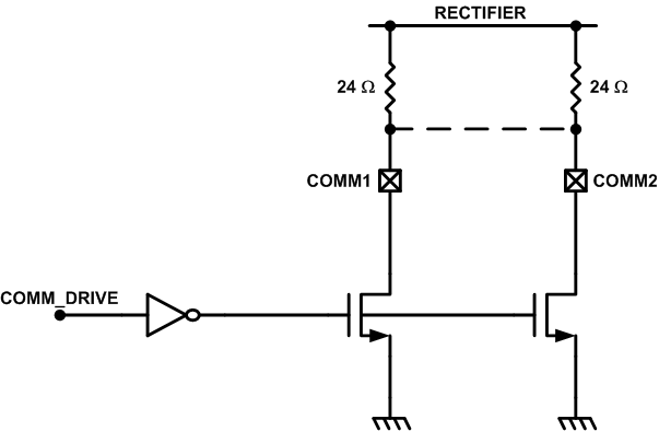
The BQ51013C-Q1 device provides two identical, integrated communication FETs which are connected to the pins COMM1 and COMM2. These FETs are used for modulating the secondary load current which allows the BQ51013C-Q1 to communicate error control and configuration information to the transmitter. Figure 8-10 shows how the COMMx pins can be used for resistive load modulation. Each COMMx pin can handle at most a 24-Ω communication resistor. Therefore, if a COMMx resistor between 12 Ω and 24 Ω is required, COMM1 and COMM2 pins must be connected in parallel. The BQ51013C-Q1 device does not support a COMMx resistor less than 12 Ω.
 Figure 8-10 Resistive
Load Modulation
Figure 8-10 Resistive
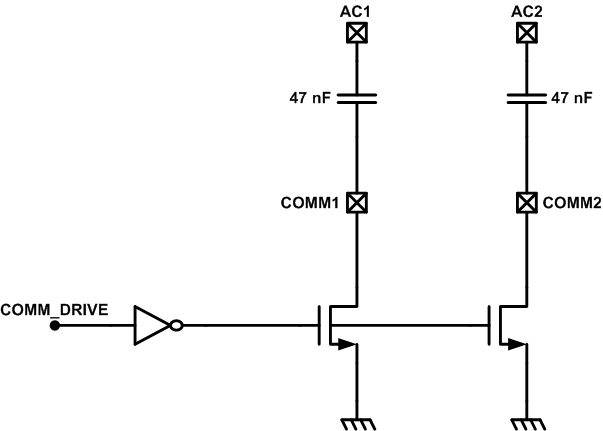
Load ModulationIn addition to resistive load modulation, the BQ51013C-Q1 is also capable of capacitive load modulation as shown in Figure 8-11. In this case, a capacitor is connected from COMM1 to AC1 and from COMM2 to AC2. When the COMMx switches are closed there is effectively a 22 nF capacitor connected between AC1 and AC2. Connecting a capacitor in between AC1 and AC2 modulates the impedance seen by the coil, which will be reflected in the primary as a change in current.
 Figure 8-11 Capacitive Load Modulation