SLUSFU9 October 2024 BQ51013C
PRODUCTION DATA
- 1
- 1 Features
- 2 Applications
- 3 Description
- 4 Description (continued)
- 5 Device Comparison Table
- 6 Pin Configuration and Functions
- 7 Specifications
-
8 Detailed Description
- 8.1 Overview
- 8.2 Functional Block Diagram
- 8.3
Feature Description
- 8.3.1 Details of a Qi Wireless Power System and BQ51013C Power Transfer Flow Diagrams
- 8.3.2 Dynamic Rectifier Control
- 8.3.3 Dynamic Efficiency Scaling
- 8.3.4 RILIM Calculations
- 8.3.5 Input Overvoltage
- 8.3.6 Adapter Enable Functionality and EN1/EN2 Control
- 8.3.7 End Power Transfer Packet (WPC Header 0x02)
- 8.3.8 Status Outputs
- 8.3.9 WPC Communication Scheme
- 8.3.10 Communication Modulator
- 8.3.11 Adaptive Communication Limit
- 8.3.12 Synchronous Rectification
- 8.3.13 Temperature Sense Resistor Network (TS)
- 8.3.14 3-State Driver Recommendations for the TS/CTRL Pin
- 8.3.15 Thermal Protection
- 8.3.16 WPC v2.0 Compliance – Foreign Object Detection
- 8.3.17 Receiver Coil Load-Line Analysis
- 8.4 Device Functional Modes
-
9 Application and Implementation
- 9.1 Application Information
- 9.2
Typical Applications
- 9.2.1
BQ51013C Wireless Power Receiver Used as a Power Supply
- 9.2.1.1 Design Requirements
- 9.2.1.2
Detailed Design Procedure
- 9.2.1.2.1 Using The BQ51013C as a Wireless Power Supply: (See Figure 1-1 )
- 9.2.1.2.2 Series and Parallel Resonant Capacitor Selection
- 9.2.1.2.3 Recommended RX Coils
- 9.2.1.2.4 COMM, CLAMP, and BOOT Capacitors
- 9.2.1.2.5 Control Pins and CHG
- 9.2.1.2.6 Current Limit and FOD
- 9.2.1.2.7 RECT and OUT Capacitance
- 9.2.1.3 Application Curves
- 9.2.2 Dual Power Path: Wireless Power and DC Input
- 9.2.3 Wireless and Direct Charging of a Li-Ion Battery at 800 mA
- 9.2.1
BQ51013C Wireless Power Receiver Used as a Power Supply
- 10Power Supply Recommendations
- 11Layout
- 12Device and Documentation Support
- 13Revision History
- 14Mechanical, Packaging, and Orderable Information
Package Options
Refer to the PDF data sheet for device specific package drawings
Mechanical Data (Package|Pins)
- RHL|20
Thermal pad, mechanical data (Package|Pins)
- RHL|20
Orderable Information
8.3.10 Communication Modulator
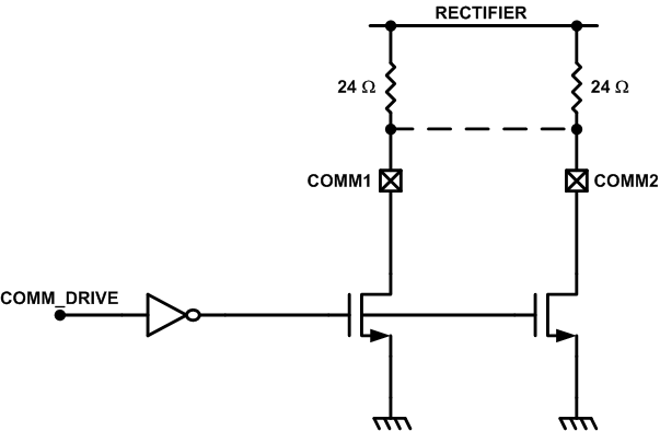
The BQ51013C device provides two identical, integrated communication FETs which are connected to the pins COMM1 and COMM2. These FETs are used for modulating the secondary load current which allows the BQ51013C to communicate error control and configuration information to the transmitter. Figure 8-10 shows how the COMMx pins can be used for resistive load modulation. Each COMMx pin can handle at most a 24-Ω communication resistor. Therefore, if a COMMx resistor between 12 Ω and 24 Ω is required, COMM1 and COMM2 pins must be connected in parallel. The BQ51013C device does not support a COMMx resistor less than 12 Ω.
 Figure 8-10 Resistive
Load Modulation
Figure 8-10 Resistive
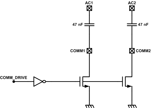
Load ModulationIn addition to resistive load modulation, the BQ51013C is also capable of capacitive load modulation as shown in Figure 8-11. In this case, a capacitor is connected from COMM1 to AC1 and from COMM2 to AC2. When the COMMx switches are closed there is effectively a 22 nF capacitor connected between AC1 and AC2. Connecting a capacitor in between AC1 and AC2 modulates the impedance seen by the coil, which will be reflected in the primary as a change in current.
 Figure 8-11 Capacitive Load Modulation