SLUSFU9 October 2024 BQ51013C
PRODUCTION DATA
- 1
- 1 Features
- 2 Applications
- 3 Description
- 4 Description (continued)
- 5 Device Comparison Table
- 6 Pin Configuration and Functions
- 7 Specifications
-
8 Detailed Description
- 8.1 Overview
- 8.2 Functional Block Diagram
- 8.3
Feature Description
- 8.3.1 Details of a Qi Wireless Power System and BQ51013C Power Transfer Flow Diagrams
- 8.3.2 Dynamic Rectifier Control
- 8.3.3 Dynamic Efficiency Scaling
- 8.3.4 RILIM Calculations
- 8.3.5 Input Overvoltage
- 8.3.6 Adapter Enable Functionality and EN1/EN2 Control
- 8.3.7 End Power Transfer Packet (WPC Header 0x02)
- 8.3.8 Status Outputs
- 8.3.9 WPC Communication Scheme
- 8.3.10 Communication Modulator
- 8.3.11 Adaptive Communication Limit
- 8.3.12 Synchronous Rectification
- 8.3.13 Temperature Sense Resistor Network (TS)
- 8.3.14 3-State Driver Recommendations for the TS/CTRL Pin
- 8.3.15 Thermal Protection
- 8.3.16 WPC v2.0 Compliance – Foreign Object Detection
- 8.3.17 Receiver Coil Load-Line Analysis
- 8.4 Device Functional Modes
-
9 Application and Implementation
- 9.1 Application Information
- 9.2
Typical Applications
- 9.2.1
BQ51013C Wireless Power Receiver Used as a Power Supply
- 9.2.1.1 Design Requirements
- 9.2.1.2
Detailed Design Procedure
- 9.2.1.2.1 Using The BQ51013C as a Wireless Power Supply: (See Figure 1-1 )
- 9.2.1.2.2 Series and Parallel Resonant Capacitor Selection
- 9.2.1.2.3 Recommended RX Coils
- 9.2.1.2.4 COMM, CLAMP, and BOOT Capacitors
- 9.2.1.2.5 Control Pins and CHG
- 9.2.1.2.6 Current Limit and FOD
- 9.2.1.2.7 RECT and OUT Capacitance
- 9.2.1.3 Application Curves
- 9.2.2 Dual Power Path: Wireless Power and DC Input
- 9.2.3 Wireless and Direct Charging of a Li-Ion Battery at 800 mA
- 9.2.1
BQ51013C Wireless Power Receiver Used as a Power Supply
- 10Power Supply Recommendations
- 11Layout
- 12Device and Documentation Support
- 13Revision History
- 14Mechanical, Packaging, and Orderable Information
Package Options
Refer to the PDF data sheet for device specific package drawings
Mechanical Data (Package|Pins)
- RHL|20
Thermal pad, mechanical data (Package|Pins)
- RHL|20
Orderable Information
8.3.9 WPC Communication Scheme
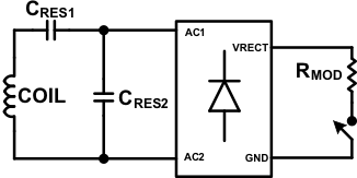
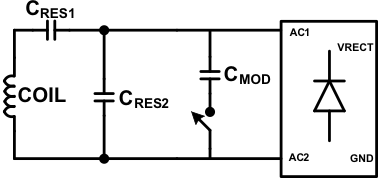
The WPC communication uses a modulation technique termed “back-scatter modulation” where the receiver coil is dynamically loaded in order to provide amplitude modulation of the transmitter's coil voltage and current. This scheme is possible due to the fundamental behavior between two loosely coupled inductors (here between the TX and RX coils). This type of modulation can be accomplished by switching in and out a resistor at the output of the rectifier, or by switching in and out a capacitor across the AC1/AC2 net. Figure 8-4 shows how to implement resistive modulation.
 Figure 8-4 Resistive Modulation
Figure 8-5 shows how to implement capacitive modulation.
 Figure 8-5 Capacitive Modulation
The amplitude change in the TX coil voltage or current can be detected by the transmitter's decoder. The resulting signal observed by the TX is shown in Figure 8-6.
 Figure 8-6 TX
Coil Voltage/Current
Figure 8-6 TX
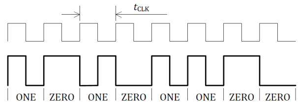
Coil Voltage/CurrentThe WPC protocol uses a differential bi-phase encoding scheme to modulate the data bits onto the TX coil voltage/current. Each data bit is aligned at a full period of 0.5 ms (tCLK) or 2 kHz. An encoded ONE results in two transitions during the bit period and an encoded ZERO results in a single transition. See Figure 8-7 for an example of the differential bi-phase encoding.
 Figure 8-7 Differential Bi-Phase Encoding Scheme (WPC Volume 1: Low Power, Part 1 Interface Definition)
The bits are sent LSB first and use an 11-bit asynchronous serial format for each portion of the packet. This includes one start bit, n-data bytes, a parity bit, and a single stop bit. The start bit is always ZERO and the parity bit is odd. The stop bit is always ONE. Figure 8-8 shows the details of the asynchronous serial format.
 Figure 8-8 Asynchronous Serial Formatting (WPC Volume 1: Low Power, Part 1 Interface
Definition)
Figure 8-8 Asynchronous Serial Formatting (WPC Volume 1: Low Power, Part 1 Interface
Definition)Each packet format is organized as shown in Figure 8-9.
 Figure 8-9 Packet Format (WPC Volume 1: Low Power, Part 1 Interface Definition)
Figure 7-20 shows an example waveform of the receiver sending a rectified power packet (header 0x04).