SWRS205F March   2017  – December 2024 CC3120MOD

PRODUCTION DATA  

  1.   1
  2. Features
  3. Applications
  4. Description
  5. Functional Block Diagrams
  6. Device Comparison
    1. 5.1 Related Products
  7. Terminal Configuration and Functions
    1. 6.1 CC3120MOD Pin Diagram
    2. 6.2 Pin Attributes
      1.      11
    3. 6.3 Connections for Unused Pins
  8. Specifications
    1. 7.1  Absolute Maximum Ratings
    2. 7.2  ESD Ratings
    3. 7.3  Recommended Operating Conditions
    4. 7.4  Current Consumption Summary
    5. 7.5  TX Power and IBAT versus TX Power Level Settings
    6. 7.6  Brownout and Blackout Conditions
    7. 7.7  Electrical Characteristics
    8. 7.8  WLAN Receiver Characteristics
    9. 7.9  WLAN Transmitter Characteristics
    10. 7.10 Reset Requirement
    11. 7.11 Thermal Resistance Characteristics for MOB Package
    12. 7.12 Timing and Switching Characteristics
      1. 7.12.1 Power-Up Sequencing
      2. 7.12.2 Power-Down Sequencing
      3. 7.12.3 Device Reset
      4. 7.12.4 Wakeup From HIBERNATE Mode Timing
    13. 7.13 External Interfaces
      1. 7.13.1 SPI Host Interface
      2. 7.13.2 Host UART Interface
        1. 7.13.2.1 5-Wire UART Topology
        2. 7.13.2.2 4-Wire UART Topology
        3. 7.13.2.3 3-Wire UART Topology
      3. 7.13.3 External Flash Interface
  9. Detailed Description
    1. 8.1 Overview
    2. 8.2 Module Features
      1. 8.2.1 WLAN
      2. 8.2.2 Network Stack
        1. 8.2.2.1 Security
      3. 8.2.3 Host Interface and Driver
      4. 8.2.4 System
    3. 8.3 Power-Management Subsystem
      1. 8.3.1 VBAT Wide-Voltage Connection
    4. 8.4 Low-Power Operating Modes
      1. 8.4.1 Low-Power Deep Sleep
      2. 8.4.2 Hibernate
      3. 8.4.3 Shutdown
    5. 8.5 Restoring Factory Default Configuration
    6. 8.6 Device Certification and Qualification
      1. 8.6.1 FCC Certification and Statement
      2. 8.6.2 Industry Canada (IC) Certification and Statement
      3. 8.6.3 ETSI/CE Certification
      4. 8.6.4 Japan MIC Certification
      5. 8.6.5 SRRC Certification and Statement
    7. 8.7 Module Markings
    8. 8.8 End Product Labeling
    9. 8.9 Manual Information to the End User
  10. Applications, Implementation, and Layout
    1. 9.1 Application Information
      1. 9.1.1 Typical Application
      2. 9.1.2 Power Supply Decoupling and Bulk Capacitors
      3. 9.1.3 Reset
      4. 9.1.4 Unused Pins
    2. 9.2 PCB Layout Guidelines
      1. 9.2.1 General Layout Recommendations
      2. 9.2.2 RF Layout Recommendations
      3. 9.2.3 Antenna Placement and Routing
      4. 9.2.4 Transmission Line Considerations
  11. 10Environmental Requirements and Specifications
    1. 10.1 Temperature
      1. 10.1.1 PCB Bending
    2. 10.2 Handling Environment
      1. 10.2.1 Terminals
      2. 10.2.2 Falling
    3. 10.3 Storage Condition
      1. 10.3.1 Moisture Barrier Bag Before Opened
      2. 10.3.2 Moisture Barrier Bag Open
    4. 10.4 Baking Conditions
    5. 10.5 Soldering and Reflow Condition
  12. 11Device and Documentation Support
    1. 11.1 Device Nomenclature
    2. 11.2 Development Tools and Software
    3. 11.3 Firmware Updates
    4. 11.4 Documentation Support
    5. 11.5 Trademarks
    6. 11.6 Electrostatic Discharge Caution
    7. 11.7 Glossary
  13. 12Revision History
  14. 13Mechanical, Packaging, and Orderable Information
    1. 13.1 Mechanical, Land, and Solder Paste Drawings
    2. 13.2 Package Option Addendum
      1. 13.2.1 Packaging Information
    3. 13.3 Tape and Reel Information
      1. 13.3.1 Tape and Reel Specification

Refer to the PDF data sheet for device specific package drawings

Mechanical Data (Package|Pins)
  • MOB|63
Thermal pad, mechanical data (Package|Pins)

Brownout and Blackout Conditions

The device enters a brownout condition when the input voltage dips below VBROWNOUT (see Figure 7-4 and Figure 7-5). This condition must be considered during design of the power supply routing, especially if operating from a battery. High-current operations, such as a TX packet or any external activity (not necessarily related directly to networking) can cause a drop in the supply voltage, potentially triggering a brownout condition. The resistance includes the internal resistance of the battery, contact resistance of the battery holder (four contacts for a 2× AA battery), and the wiring and PCB routing resistance.

Note:

When the device is in the Hibernate state, brownout is not detected; only blackout is in effect during the Hibernate state.
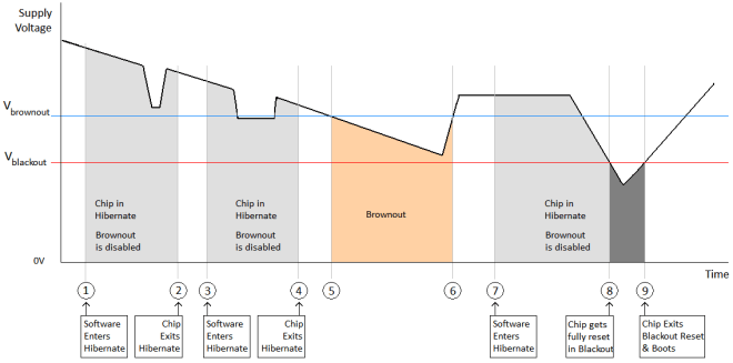
CC3120MOD Brownout and Blackout Levels (1 of 2)Figure 7-4 Brownout and Blackout Levels (1 of 2)
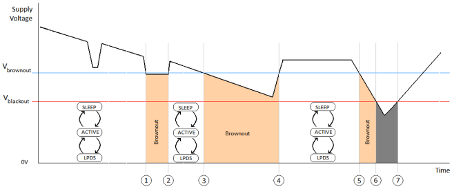
 

CC3120MOD Brownout and Blackout Levels (2 of 2)Figure 7-5 Brownout and Blackout Levels (2 of 2)


In the brownout condition, all sections of the CC3120MOD (including the 32kHz RTC) shut down except for the Hibernate module, which remains on. The current in this state can reach approximately 400µA. The blackout condition is equivalent to a hardware reset event in which all states within the device are lost.

Table 7-1 lists the brownout and blackout voltage levels.

Table 7-1 Brownout and Blackout Voltage Levels
CONDITIONVOLTAGE LEVELUNIT
Vbrownout2.1V
Vblackout1.67V