SCHS047M August 1998 – November 2024 CD4051B , CD4052B , CD4053B
PRODUCTION DATA
- 1
- 1 Features
- 2 Applications
- 3 Description
- 4 Pin Configuration and Functions
- 5 Specifications
- 6 Parameter Measurement Information
- 7 Detailed Description
- 8 Application and Implementation
- 9 Device and Documentation Support
- 10Revision History
- 11Mechanical, Packaging, and Orderable Information
Package Options
Mechanical Data (Package|Pins)
- J|16
Thermal pad, mechanical data (Package|Pins)
Orderable Information
4 Pin Configuration and Functions
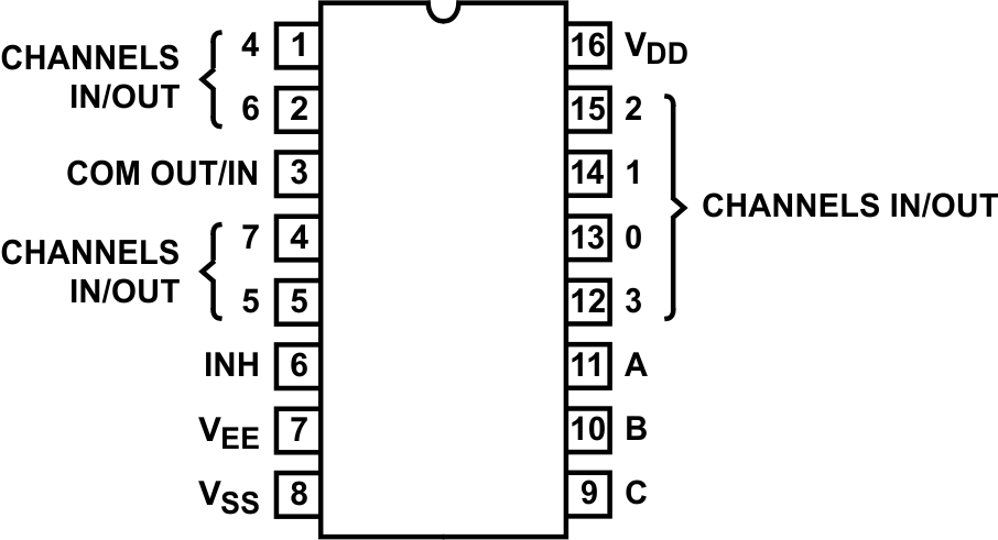
 Figure 4-1 CD4051B E, M, NS, and PW Package,16-Pin PDIP, CDIP, SOIC, SOP, and
TSSOP(Top View)
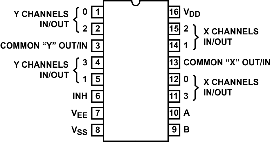
 Figure 4-2 CD4052B E, M, NS, and PW Package,16-Pin PDIP, CDIP, SOP, and TSSOP(Top View)
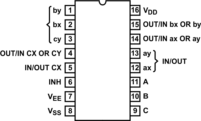
 Figure 4-3 CD4053B E, M, NS,
and PW Package,16-Pin PDIP, CDIP, SOP,
and TSSOP
(Top View)
Figure 4-3 CD4053B E, M, NS,
and PW Package,16-Pin PDIP, CDIP, SOP,
and TSSOP
(Top View)Table 4-1 Pin Functions CD4051B
| PIN | TYPE(1) | DESCRIPTION | |||||
|---|---|---|---|---|---|---|---|
| NO. | NAME | ||||||
| 1 | CH 4 IN/OUT | I/O | Channel 4 in/out | ||||
| 2 | CH 6 IN/OUT | I/O | Channel 6 in/out | ||||
| 3 | COM OUT/IN | I/O | Common out/in | ||||
| 4 | CH 7 IN/OUT | I/O | Channel 7 in/out | ||||
| 5 | CH 5 IN/OUT | I/O | Channel 5 in/out | ||||
| 6 | INH | I | Disables all channels. See Table 7-1. | ||||
| 7 | VEE | — | Negative power input | ||||
| 8 | VSS | — | Ground | ||||
| 9 | C | I | Channel select C. See Table 7-1. | ||||
| 10 | B | I | Channel select B. See Table 7-1. | ||||
| 11 | A | I | Channel select A. See Table 7-1. | ||||
| 12 | CH 3 IN/OUT | I/O | Channel 3 in/out | ||||
| 13 | CH 0 IN/OUT | I/O | Channel 0 in/out | ||||
| 14 | CH 1 IN/OUT | I/O | Channel 1 in/out | ||||
| 15 | CH 2 IN/OUT | I/O | Channel 2 in/out | ||||
| 16 | VDD | — | Positive power input | ||||
(1) I = input, O = output
Table 4-2 Pin Functions CD4052B
| PIN | TYPE(1) | DESCRIPTION | |||||
|---|---|---|---|---|---|---|---|
| NO. | NAME | ||||||
| 1 | Y CH 0 IN/OUT | I/O | Channel Y0 in/out | ||||
| 2 | Y CH 2 IN/OUT | I/O | Channel Y2 in/out | ||||
| 3 | Y COM OUT/IN | I/O | Y common out/in | ||||
| 4 | Y CH 3 IN/OUT | I/O | Channel Y3 in/out | ||||
| 5 | Y CH 1 IN/OUT | I/O | Channel Y1 in/out | ||||
| 6 | INH | I | Disables all channels. See Table 7-1. | ||||
| 7 | VEE | — | Negative power input | ||||
| 8 | VSS | — | Ground | ||||
| 9 | B | I | Channel select B. See Table 7-1. | ||||
| 10 | A | I | Channel select A. See Table 7-1. | ||||
| 11 | X CH 3 IN/OUT | I/O | Channel X3 in/out | ||||
| 12 | X CH 0 IN/OUT | I/O | Channel X0 in/out | ||||
| 13 | X COM IN/OUT | I/O | X common out/in | ||||
| 14 | X CH 1 IN/OUT | I/O | Channel in/out | ||||
| 15 | X CH 2 IN/OUT | I/O | Channel in/out | ||||
| 16 | VDD | — | Positive power input | ||||
(1) I = input, O = output
Table 4-3 Pin Functions CD4053B
| PIN | TYPE(1) | DESCRIPTION | |||||
|---|---|---|---|---|---|---|---|
| NO. | NAME | ||||||
| 1 | BY IN/OUT | I/O | B channel Y in/out | ||||
| 2 | BX IN/OUT | I/O | B channel X in/out | ||||
| 3 | CY IN/OUT | I/O | C channel Y in/out | ||||
| 4 | CX OR CY OUT/IN | I/O | C common out/in | ||||
| 5 | CX IN/OUT | I/O | C channel X in/out | ||||
| 6 | INH | I | Disables all channels. See Table 7-1. | ||||
| 7 | VEE | — | Negative power input | ||||
| 8 | VSS | — | Ground | ||||
| 9 | C | I | Channel select C. See Table 7-1. | ||||
| 10 | B | I | Channel select B. See Table 7-1. | ||||
| 11 | A | I | Channel select A. See Table 7-1. | ||||
| 12 | AX IN/OUT | I/O | A channel X in/out | ||||
| 13 | AY IN/OUT | I/O | A channel Y in/out | ||||
| 14 | AX OR AY OUT/IN | I/O | A common out/in | ||||
| 15 | BX OR BY OUT/IN | I/O | B common out/in | ||||
| 16 | VDD | — | Positive power input | ||||
(1) I = input, O = output