SCHS047M August   1998  – November 2024 CD4051B , CD4052B , CD4053B

PRODUCTION DATA  

  1.   1
  2. Features
  3. Applications
  4. Description
  5. Pin Configuration and Functions
  6. Specifications
    1. 5.1 Absolute Maximum Ratings
    2. 5.2 ESD Ratings
    3. 5.3 Recommended Operating Conditions
    4. 5.4 Thermal Information
    5. 5.5 Electrical Characteristics
    6. 5.6 AC Performance Characteristics
    7. 5.7 Typical Characteristics
  7. Parameter Measurement Information
  8. Detailed Description
    1. 7.1 Overview
    2. 7.2 Functional Block Diagrams
    3. 7.3 Feature Description
    4. 7.4 Device Functional Modes
  9. Application and Implementation
    1. 8.1 Application Information
    2. 8.2 Typical Application
      1. 8.2.1 Design Requirements
      2. 8.2.2 Detailed Design Procedure
      3. 8.2.3 Application Curve
    3. 8.3 Power Supply Recommendations
    4. 8.4 Layout
      1. 8.4.1 Layout Guidelines
      2. 8.4.2 Layout Example
  10. Device and Documentation Support
    1. 9.1 Documentation Support
      1. 9.1.1 Related Documentation
    2. 9.2 Receiving Notification of Documentation Updates
    3. 9.3 Support Resources
    4. 9.4 Trademarks
    5. 9.5 Electrostatic Discharge Caution
    6. 9.6 Glossary
  11. 10Revision History
  12. 11Mechanical, Packaging, and Orderable Information

Package Options

Mechanical Data (Package|Pins)
Thermal pad, mechanical data (Package|Pins)
Orderable Information

Functional Block Diagrams

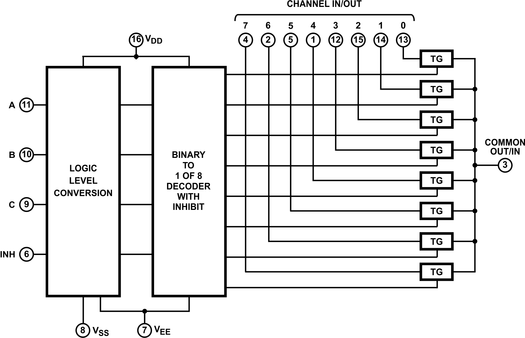
CD4051B CD4052B CD4053B Functional Block Diagram, CD4051B
All inputs are protected by standard CMOS protection network.
Figure 7-1 Functional Block Diagram, CD4051B
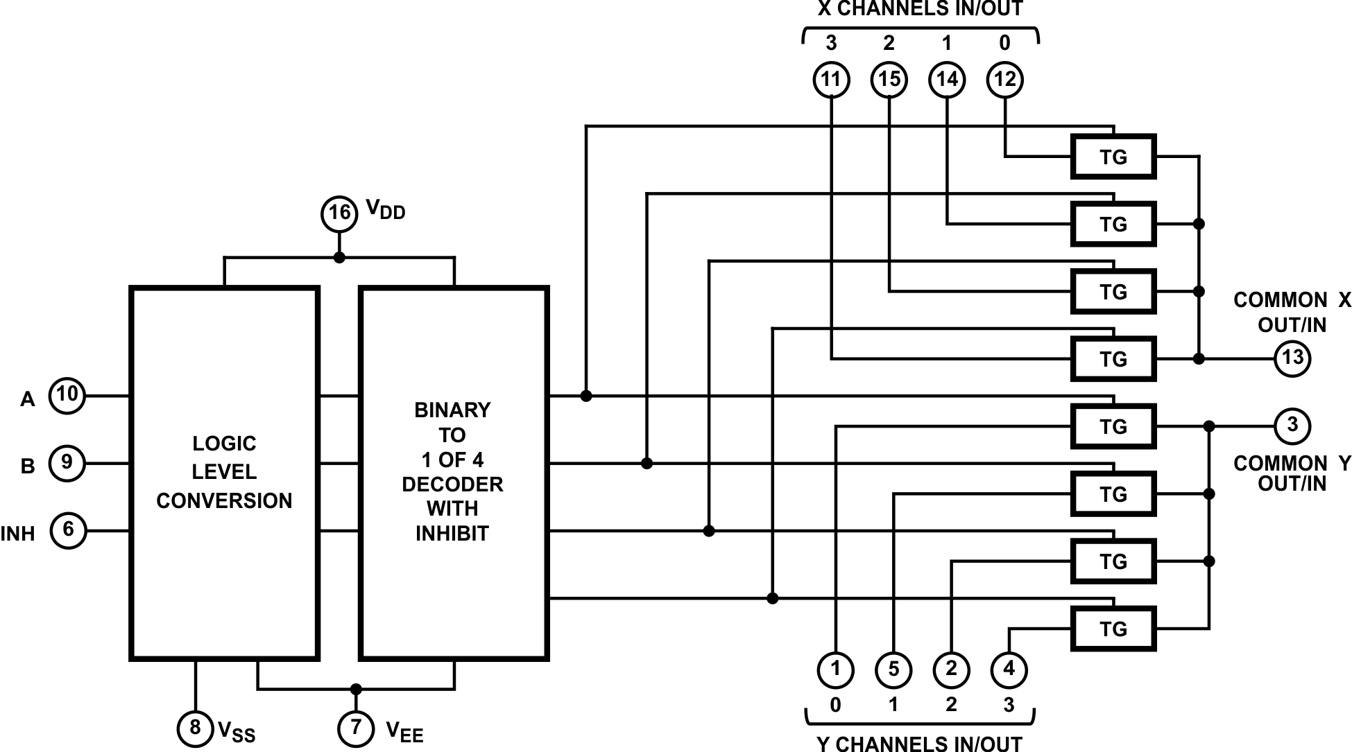
CD4051B CD4052B CD4053B Functional Block Diagram, CD4052B
All inputs are protected by standard CMOS protection network.
Figure 7-2 Functional Block Diagram, CD4052B
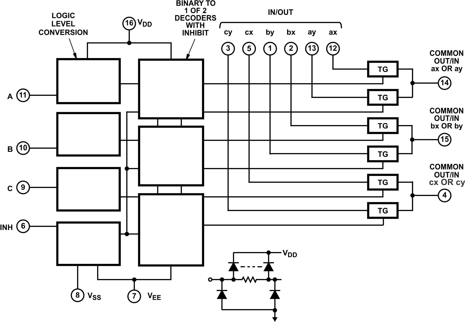
CD4051B CD4052B CD4053B Functional Block Diagram, CD4053B
All inputs are protected by standard CMOS protection network.
Figure 7-3 Functional Block Diagram, CD4053B