SCAS918E June 2013 – August 2024 CDCE913-Q1 , CDCEL913-Q1
PRODUCTION DATA
- 1
- 1 Features
- 2 Applications
- 3 Description
- 4 Device Comparison
- 5 Pin Configuration and Functions
- 6 Specifications
- 7 Parameter Measurement Information
- 8 Detailed Description
- 9 Application and Implementation
- 10Register Maps
- 11Device and Documentation Support
- 12Revision History
- 13Mechanical, Packaging, and Orderable Information
Package Options
Mechanical Data (Package|Pins)
- PW|14
Thermal pad, mechanical data (Package|Pins)
Orderable Information
3 Description
The CDCE913-Q1 and CDCEL913-Q1 devices are modular, phase-locked loop (PLL)-based programmable clock synthesizers. These devices provide flexible and programmable options, such as output clocks, input signals, and control pins, so that the user can configure the CDCE913-Q1 and CDCEL913-Q1 for their own specifications.
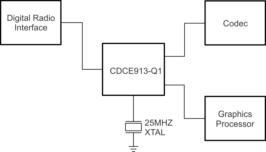
The CDCE913-Q1 and CDCEL913-Q1 generate up to three output clocks from a single input frequency to enable both board space and cost savings. Additionally, with multiple outputs, the clock generator can replace multiple crystals with one clock generator. This makes the device well-suited for head unit and telematics applications in infotainment and camera systems in ADAS, as these platforms are evolving into smaller and more cost effective systems.
Also, each output can be programmed in-system for any clock frequency up to 230MHz through the integrated, configurable PLL. The PLL also supports spread-spectrum clocking (SSC) with programmable down and center spread. This provides better electromagnetic interference (EMI) performance to enable customers to pass industry standards such as CISPR-25.
Customization of frequency programming and SSC are accessed using three, user-defined control pins. This eliminates the need to use an additional interface to control the clock. Specific power-up and power-down sequences can also be defined to the user’s needs.
| PART NUMBER | PACKAGE(1) | PACKAGE SIZE(2) |
|---|---|---|
| CDCE913-Q1 | PW (TSSOP, 14) | 5mm × 6.4mm |
| CDCEL913-Q1 |
 Simplified Schematic